Week 8
Input Devices
Step Response
I started this week by trying to make a step response input. My goal is to make a few different types of buttons (that will eventually fit in my alarm clock) using the step response input and different vinyl cutter shapes.
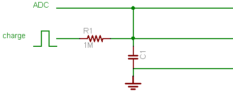
Here is a schematic of how the step response input works. The microcontroller outputs a pulse through the charge pin. The contact and the resistor form an RC network that causes a charging delay at the ADC pin. The microcontroller runs ADC conversions to measure the charging delay, which is related to the size of the parasitic capacitance. The charge signal is also sent out with the ADC signal and GND as a shield.
I made the hello.step.45.cad board with the modela and had no issues stuffing the parts. After installing gavrasm on my PC, I was able to compile and program hello.step.45.asm on the tiny45.
It took me a while to figure out how to use the Python script on my Windows PC. First, I had to install the latest version of Python. Then I needed to download and install two extra modules for python: pyserial and pywin32. After installing these modules, the hello.45.step.py program ran successfully.
Note: It is useful to update your Windows path to include the Python (and Gavrasm) directory. You do this by right clicking My Computer -> Properties -> Advanced -> Environment Variables.
So the single input version seemed to work ok. When I touched the wire going to the ADC input the response changed. My next goal was to make a slider switch. I figured I would need an input for two triangular contacts, so I made a board with two step inputs. Unfortunately, I didn't connect the second input to an ADC pin, as pointed out by Charlie. I re-made the two input board using pins 6 and 7 as the charge and ADC inputs, respectively.
When I first tested this board, I just programmed Neil's hello.step.45.asm code to check that the first input was working. It wasn't. After a while of debugging and not finding anything, I decided to replace the tiny45. This did the trick and the first input worked as expected.
Next, I tried to test the second input by changing the assembly code so that the charging pin was PB1 and the ADC input was ADC1. When I loaded up the python script I only got a flat line. I realized that the ADC input pin I was using was the same pin that I was using to transmit data back to the serial port.
I did some board surgery to move my ADC input from ADC1 to ADC2 for the second input. This means that I also had to move the charging pin for the first input from PB4/ADC2 to PB0.
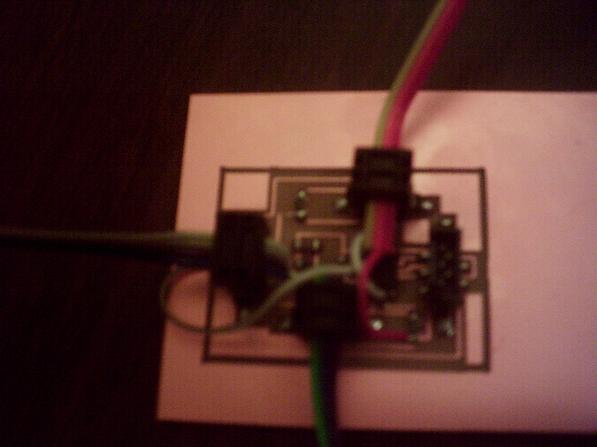
I tested this board in a similar fashion and each input functioned separately, so I knew the hardware was ok.
The next major step was figuring out the assembly and python code. Siggi helped me a lot during this, especially in explaining the assembly code and how framing worked with serial transmission. The code was adapted from hello.step.45.asm; the major changes included adding another charge bit, changing the ADCMUX, and adding a second ADC conversion for the second input. After quite a bit of debugging and timing issues we came up with the following code:
Assembly:
; loop for 1st input
   loop1:
      cbi ADMUX, MUX3 ; set MUX to ADC3
      cbi ADMUX, MUX2 ; "
      sbi ADMUX, MUX1 ; "
      sbi ADMUX, MUX0 ; "

      ldi delay_count, 254
         ;
	 ; settle sample and start upward step response (1st input)
	 ;
         cbi PORTB, charge_pin1
         rcall settle
	 mov temp, delay_count
         sbi PORTB, charge_pin1
	 ;
         ; wait for delay
	 ;
	 addelayup1:
	    dec temp
	    brne addelayup1
         ;
	 ; read response
	 ;
         sbi ADCSRA, ADSC ; start conversion
         adloopup1:
            sbic ADCSRA, ADSC ; loop until complete
            rjmp adloopup1
	 ;
	 ; save conversion
	 ;
         in uplo1, ADCL ; get low byte
         in uphi1, ADCH ; get high byte
         ;
	 ; settle sample and start downward step response (1st input)
	 ;
         rcall settle
	 mov temp, delay_count
         cbi PORTB, charge_pin1
	 ;
         ; wait for delay
	 ;
	 addelaydown1:
	    dec temp
	    brne addelaydown1
         ;
	 ; read response
	 ;
         sbi ADCSRA, ADSC ; start conversion
         adloopdown1:
            sbic ADCSRA, ADSC ; loop until complete
            rjmp adloopdown1
	 ;
	 ; send conversions
	 ;
         in txbyte, ADCL ; low down byte
         rcall putchar
         in txbyte, ADCH ; hi down byte
         rcall putchar
         mov txbyte, uplo1 ; low up byte
         rcall putchar
         mov txbyte, uphi1 ; hi up byte
         rcall putchar
         rcall char_delay

; loop for 2nd input
   loop2:
      cbi ADMUX, MUX3 ; set MUX to ADC2
      cbi ADMUX, MUX2 ; "
      sbi ADMUX, MUX1 ; "
      cbi ADMUX, MUX0 ; "

      ldi delay_count, 254
         ;
	 ; settle sample and start upward step response (2nd input)
	 ;
         cbi PORTB, charge_pin2
         rcall settle
	 mov temp, delay_count
         sbi PORTB, charge_pin2
	 ;
         ; wait for delay
	 ;
	 addelayup2:
	    dec temp
	    brne addelayup2
         ;
	 ; read response
	 ;
         sbi ADCSRA, ADSC ; start conversion
         adloopup2:
            sbic ADCSRA, ADSC ; loop until complete
            rjmp adloopup2
	 ;
	 ; save conversion
	 ;
         in uplo2, ADCL ; get low byte
         in uphi2, ADCH ; get high byte
         ;
	 ; settle sample and start downward step response (2nd input)
	 ;
         rcall settle
	 mov temp, delay_count
         cbi PORTB, charge_pin2
	 ;
         ; wait for delay
	 ;
	 addelaydown2:
	    dec temp
	    brne addelaydown2
         ;
	 ; read response
	 ;
         sbi ADCSRA, ADSC ; start conversion
         adloopdown2:
            sbic ADCSRA, ADSC ; loop until complete
            rjmp adloopdown2
	 ;
	 ; send conversions
	 ;
         in txbyte, ADCL ; low down byte
         rcall putchar
         in txbyte, ADCH ; hi down byte
         rcall putchar
         mov txbyte, uplo2 ; low up byte
         rcall putchar
         mov txbyte, uphi2 ; hi up byte
         rcall putchar
         rcall char_delay
      ;
      ; send 1 2 3 4 for framing
      ;
      ldi txbyte, 1
      rcall putchar
      ldi txbyte, 2
      rcall putchar
      ldi txbyte, 3
      rcall putchar
      ldi txbyte, 4
      rcall putchar

      rjmp loop1
Python:
import serial
#
# open serial port
#
ser = serial.Serial('com2',9600)
ser.setDTR()
ser.flush()

#
# find framing
#
byte2 = 0
byte3 = 0
byte4 = 0

value1 = 0
value2 = 0


while 1:
	while 1:
		byte1 = byte2
		byte2 = byte3
		byte3 = byte4
		byte4 = ord(ser.read())
		if ((byte1 == 1) & (byte2 == 2) & (byte3 == 3) & (byte4 == 4)):
			break
	downlo = ord( ser.read() )
	downhi = ord( ser.read() )
	uplo = ord( ser.read() )
	uphi = ord( ser.read() )
	value_up = uphi*256+uplo
	value_down = downhi*256+downlo

	value1 = (value_up + (1023-value_down))/2.0

	downlo = ord( ser.read() )
	downhi = ord( ser.read() )
	uplo = ord( ser.read() )
	uphi = ord( ser.read() )
	value_up = uphi*256+uplo
	value_down = downhi*256+downlo

	value2 = (value_up + (1023-value_down))/2.0

	print "Value1=%f\tValue2=%f"%(value1, value2)

	slider_value = 100*(value1 - value2) / (value1 + value2)

	print "Slider value = %f"%slider_value
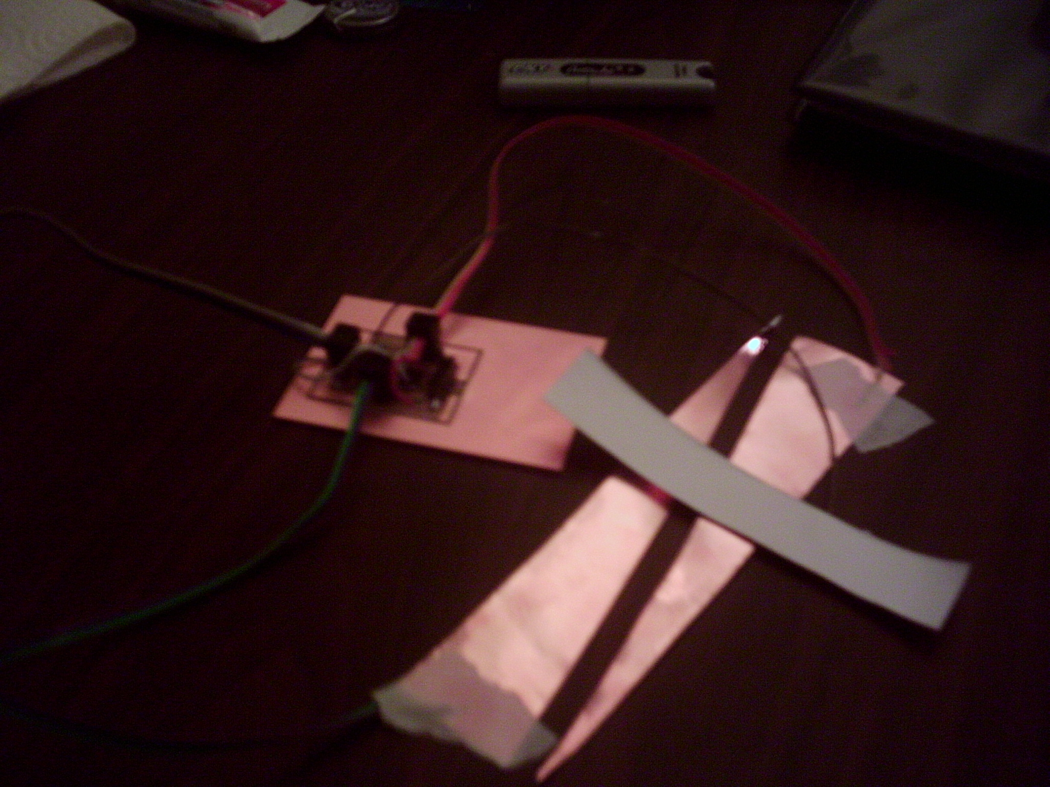
This code outputs the end values of each step response input (the ADC conversion after a delay of 254). When I touched either of the wires, these numbers changed, so everything was looking good. Next I cut two triangular pieces of copper to try out the slider. Once I hooked everything up, changing the position of the ground plate (or my finger) didn't really have any effect on the values for each of the step inputs. I am not sure how to fix this, and I don't understand why I didn't see a difference as I moved the plate across the triangles. Here is the entire test setup: