PCB Design, Fabrication, Assembly
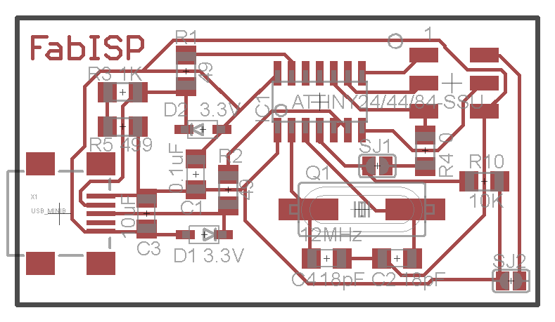
Our assignment: fabricate and assemble a PCB that would serve as our ISP (In System Programmer) for the rest of the semester. We received a premade PCB design in the form of a .PNG file
and did not need to design the PCB itself.
Milling - Getting the Modela to work its magic
When I arrived at the CBA lab, someone was already using the Modela to mill their board. I waited patiently until the end of the process and........
the PCB was not completed correctly. After a short investigation the following was concluded:
1. The board was probably not leveled on the sacrificial layer. It seems that some of the FR1 boards we received were a little curved.
2. The Z depth was not configured deep enough and as a result some of the PCB traces were not isolated from the surrounding surface
I noticed my PCB was "wavy" as well, so I replaced it with a new one that looked flat. In addition I configured the modela to cut a little deeper so that my PCB would not suffer the same fate as the previous one.
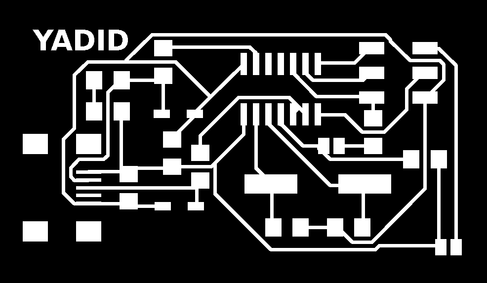
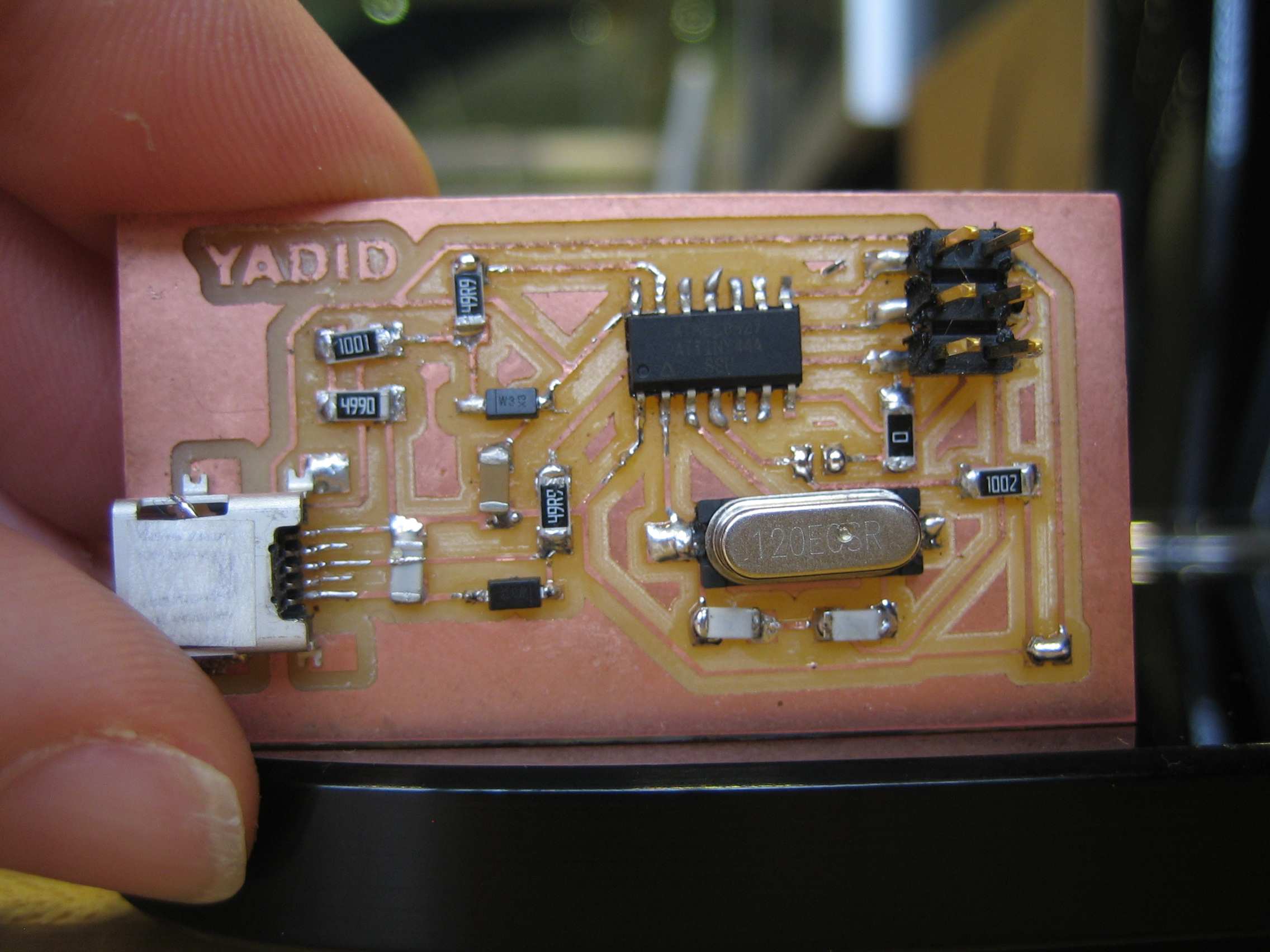
In addition, I also edited the original PCB PNG file and replaced the "ISP" wording with my name. My reasoning was, that everyone would know that this was an In System Programmer (this was obvious),
but no one could guess that it was mine - so I had it branded.
After sending my design to the modela via the command line and a few minutes of buzzing, the PCB was ready. Isued a metal shear to cut out the PCB, instead of the Modela, because it was a lot faster (I wanted to free the machine for other people to use).
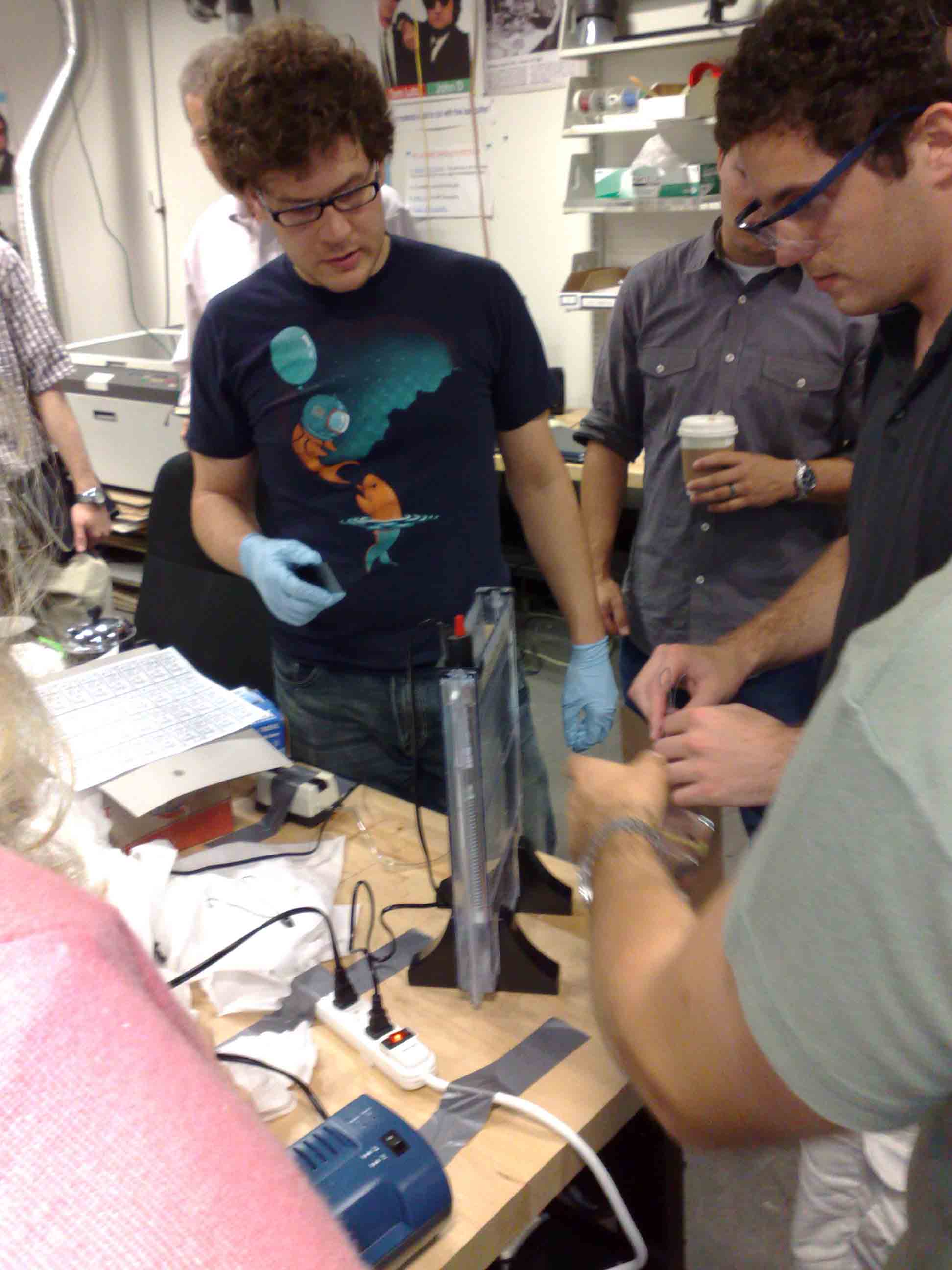
Soldering
A great tutorial on soldering can be found here.
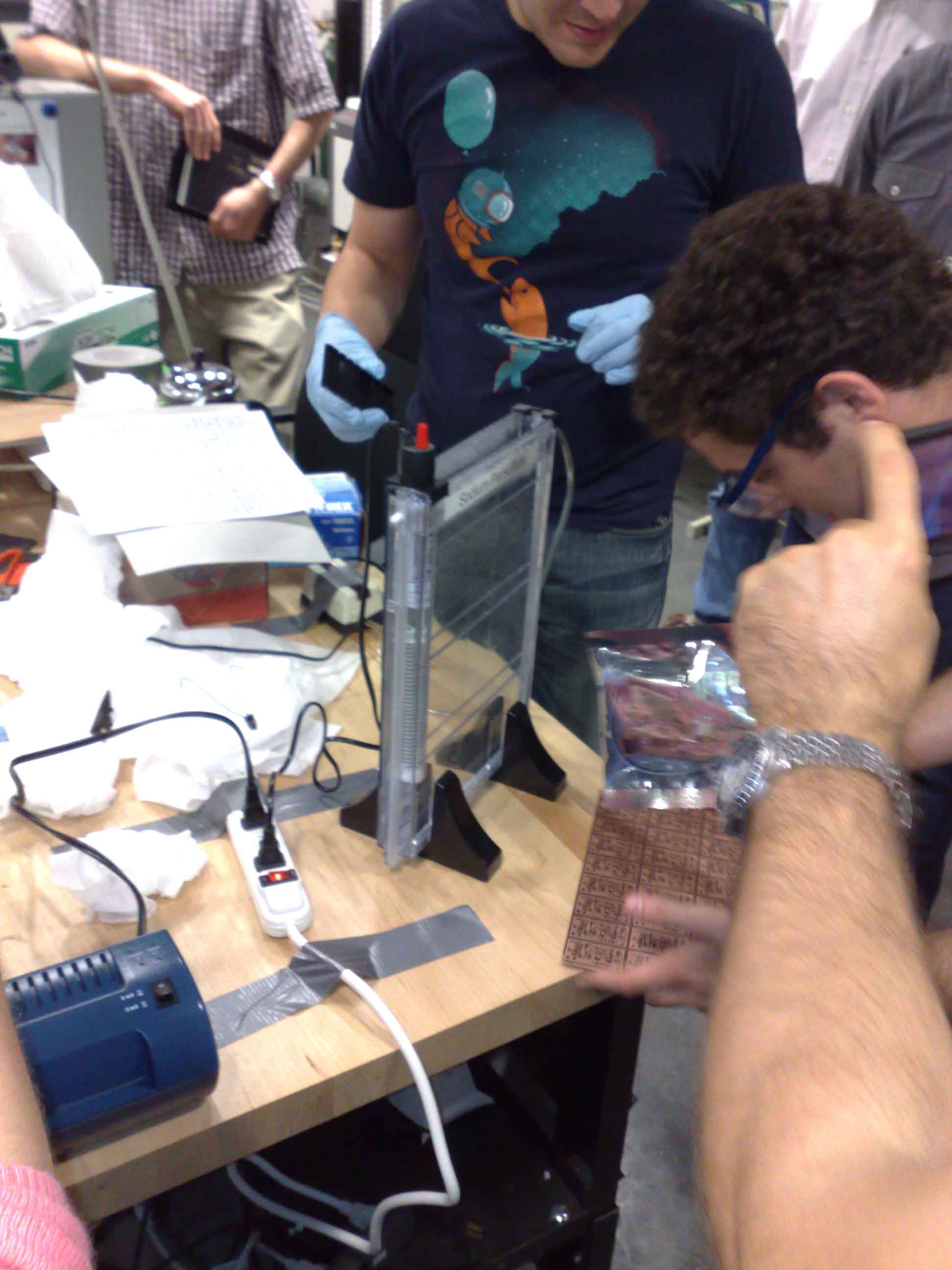
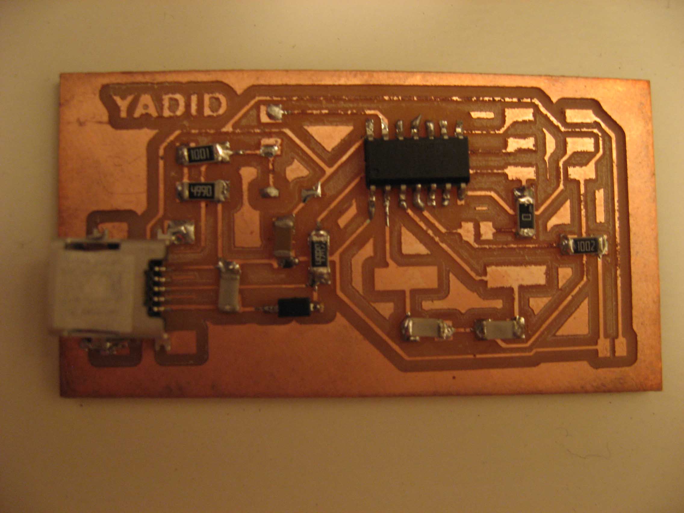
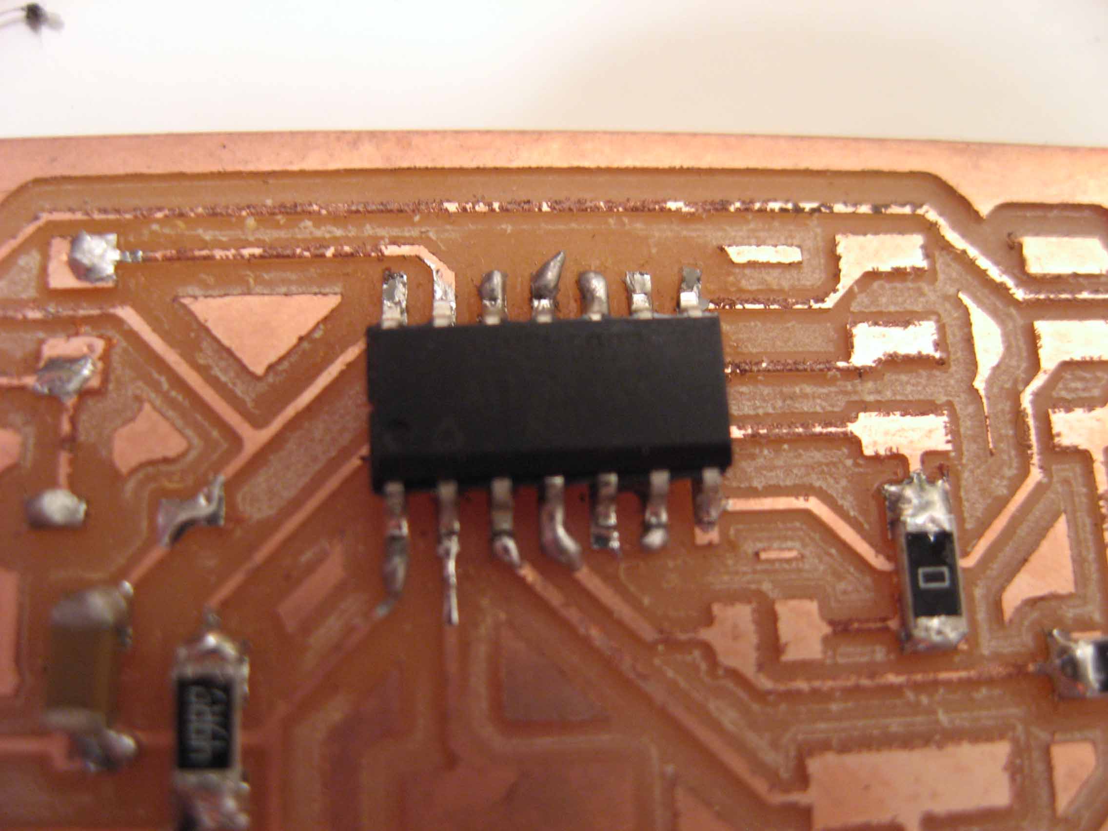
This was my first attempt at stuffing a board. In the past, I had soldered the occasional disconnected wire, but never a full board with such delicate components.
As you can see from the pictures above, my soldering technique is still somewhat sloppy but I felt an improvement throughout the process.
After I completed the soldering, I tested each connection with a multimeter and found some parts that were not soldered correctly.
After a quick soldering session to fix these I was able to program my board using another ISP which means - SUCCESS !!
My tips for soldering:
1. Start with the small parts which require few connections first. By the time you reach the micro controller and the USB you will be glad that you practiced as these have very thin wires.
2. For parts with many pads (such as USB), first anchor the part by soldering one of the corner pads which are easier to access. This will prevent the part from moving and you can solder the rest of the pads.
3. Always heat both the surface and the wire of the part. The solder will flow towards them if they are heated.
4. Make sure you clean the tip of your solder iron regularly - otherwise it will not conduct heat and you will have a hard time soldering.
If you follow these, you should be able to stuff a board easily.
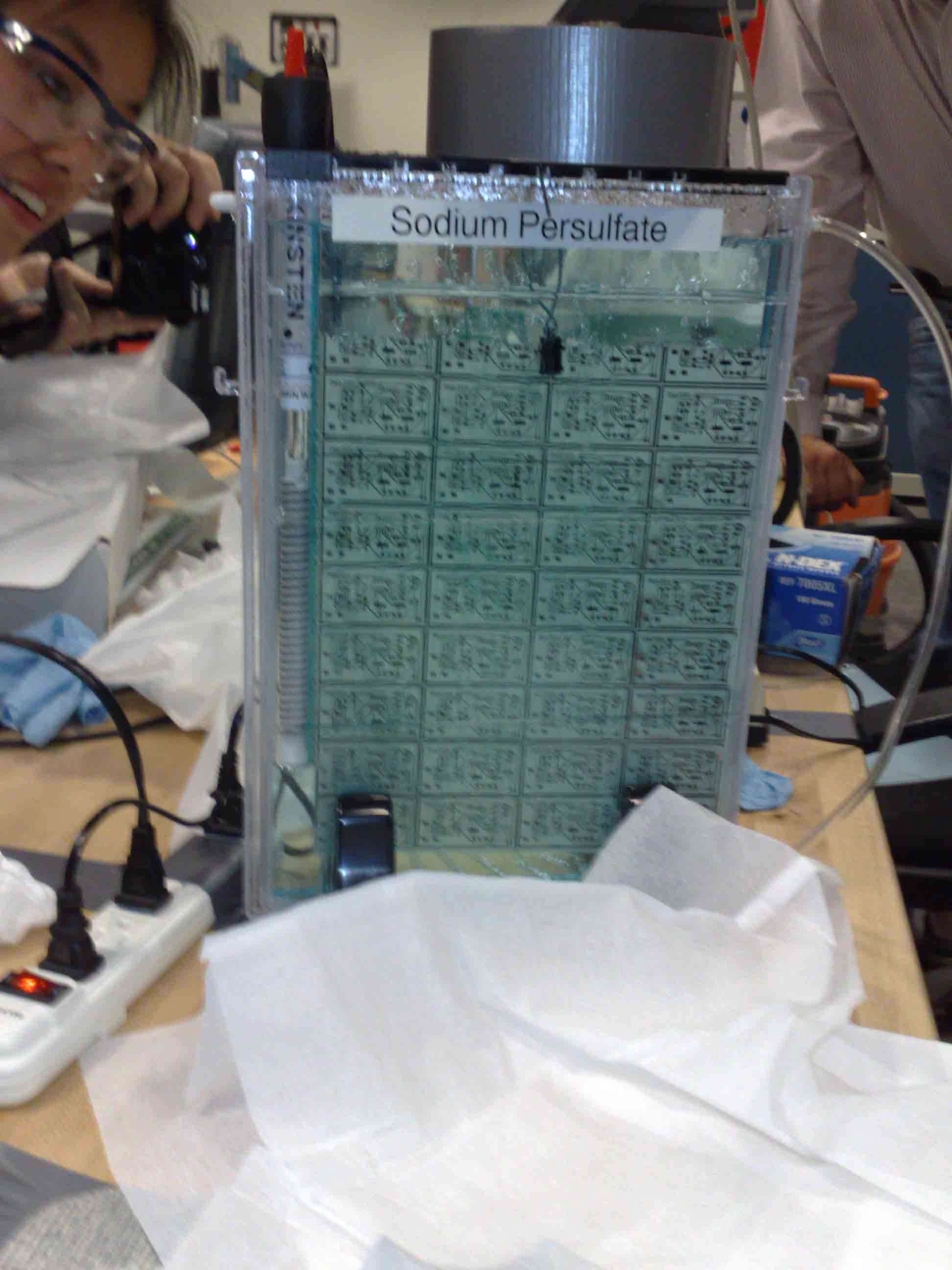
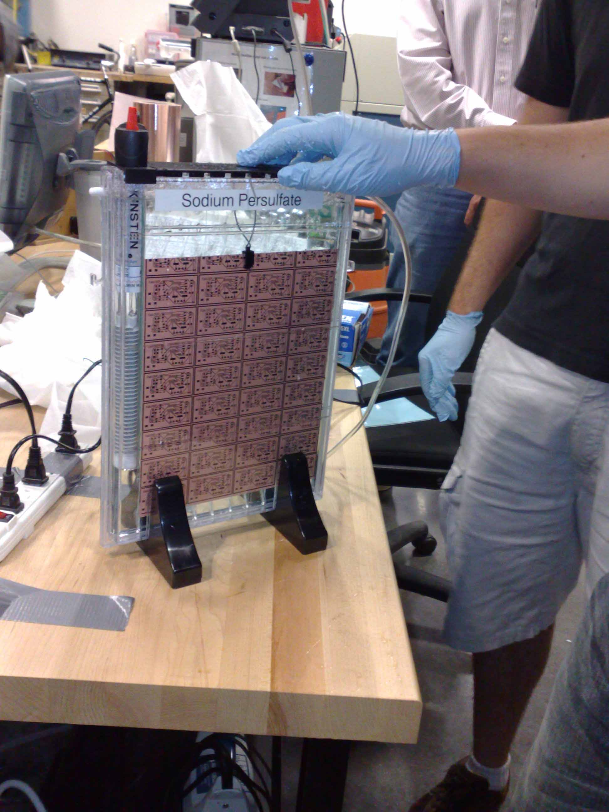
Board Etching - It really works !!!!
The TAs showed us the magic of etching PCBs. Though this process is not environment friendly, it can create Large PCBs (or multiple copies of the same PCB) very quickly.
In this process, the (mirror image of the) design is prined in a special transparency with sugar coating and then laminated to the PCB. The PCB should be very cleen, so it is rinsed with soap and water prior to the lamination.
After laminating, the PCB is put in a tank of Sodium Persulfate which is preheated to a specific temperature. After 5 minutes or so the etching has completed and the PCB is washed in cold water, which melts away the transparency.
And there you have it - an etched PCB.