Etching Tutorial
Etching: a “subtractive” method used for the production of printed circuit boards
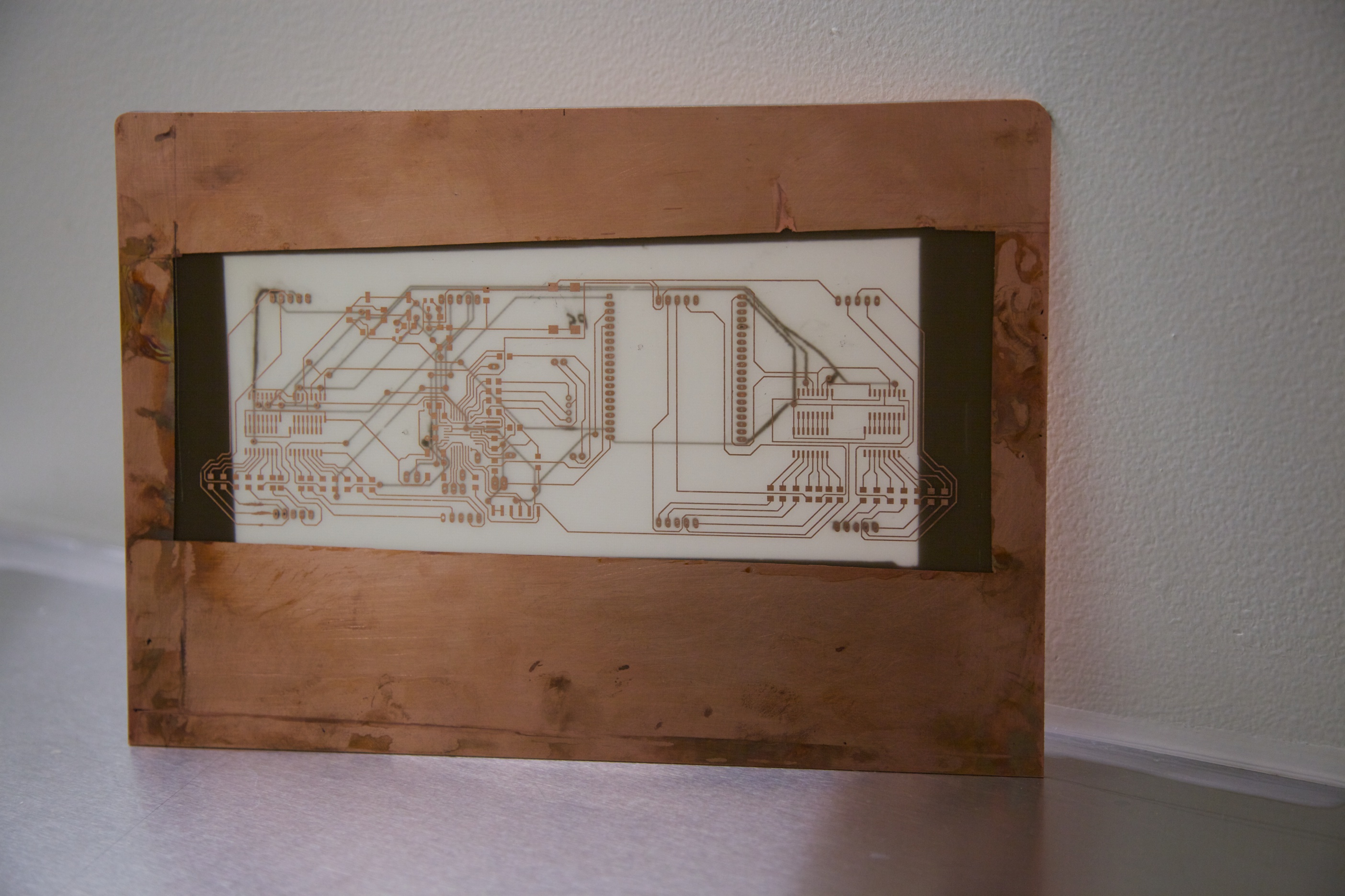
Etching is a very quick process to make PCBs and my preference. It allows you to make boards larger than what you can do with the modella, it allows you to use materials that you can’t mill (FB4) and it’s also much quicker. The total process time to etch a double sided board on 9″ x 6″ of FB4 is less than 30 minutes.
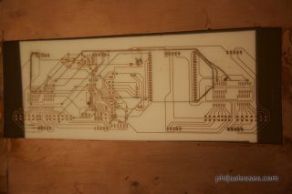
Cleaning the Board
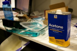
To start, clean the copper board. Wearing gloves, take acetone and a brillo pad to rough up the copper plate on both sides. This is done to take off the layer of copper that has slightly oxidized. You’ll see a color difference when you do this. Make the entire board on both sides look like the ‘new’ copper. Any areas that have oxidation will cause problems so be thorough. While scrubbing, rinse off the “gunk” using more acetone. When the board looks clean, rinse the entire plate with acetone on both sides. Run under water to rinse off acetone.
 Next, take dish soap and scrub both sides. You can do this by applying the soap directly to both sides and rub in with your gloves. This will get rid of any oil on the board. Rinse it well with water. Do this step twice to remove any oil. Rinse under water again to remove any trace of soap.
Finally, rinse the entire board with isopropyl alcohol. The alcohol will take away any remaining residue left over from the previous chemicals. When both sides are rinsed with alcohol, run the entire board under water to remove the alcohol.
At this point, it is crucial that nothing touches the board where the transfer is to be made. Prop the board up against something to let it dry. Be sure nothing touches either face.
Printing the Transfer
You should have a schematic in Eagle created. You can export the top and bottom layers of your circuit as a monotone png with 1200dpi. Next, open both the front and back circuits in photoshop as separate layers in the same file. Invert both layers so that the traces of the circuit are black. Mirror the top layer only. Using photoshop, this can be done using Transform>Flip Vertically.
Move the top layer, so that it lines up with the bottom layer manually. Once this is done, add three registration holes to an area on the board that has no traces near it on both sides. Hide the bottom layer, and print the top circuit on a piece of paper. Now hide the top layer and print the bottom circuit layer on another piece of paper. When both sheets are printed, overlay them and hold them up to the light so you can be sure that everything is printing appropriately and that everything is lined up. It is possible I messed up a step here, but the gist is simple. When you transfer the paper to the copper board, it will need to be mirrored. The one on the back side does not need to be mirrored, since it’s on a side that is already mirrored in itself. Make sure alignment holes are matching up.
When everything is good, print on to the transfer paper in the highest resolution the printer will print. This should be >1000dpi to get better ink coverage. Also, you must use a printer that has toner, since it’s made of plastic. This plastic will protect the copper board from reacting with the chemicals later.
Aligning the Circuit to the Board
This is simple. On both transfer sheets, cut out the holes with an exacto knife. Now tape down the top circuit so it can’t move.
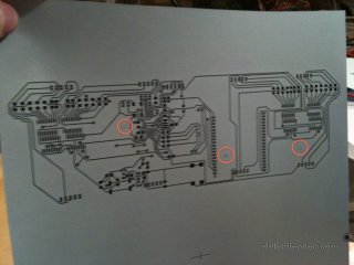
With a drill press, drill holes through the board where the registration holes are located. This will allow you to line up the holes on the other side of the board.
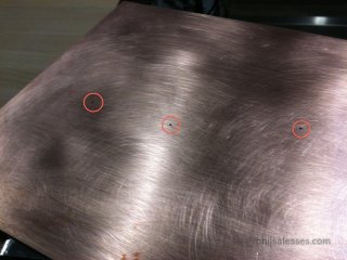
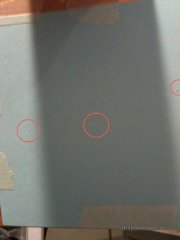
Now position the back circuit transfer with the holes. Tape both down. When you’re done, you should be able to see straight through the board where the holes are, ensuring proper alignment.
Laminator
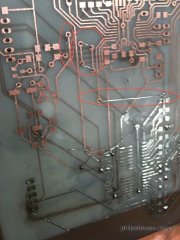
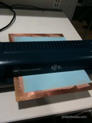
The laminator is a crucial step. It’s preferred over a manual method such as ironing due to it’s even speed and pressure. By hand ironing, it can mess things up quickly (see some improper transfer photos). Run the board through the laminator 4-6 times, melting the toner on to the copper board. When you’re done, immediately place the board in to a sheet of water. It should make a sizzle noise as the hot copper board rapidly cools. Do not touch the sheet until the paper dissolves. This should happen in about 10 minutes. You should notice bubbles have formed in the paper.
Etching
Get with a TA to help you set up the etching station. You should have etching solution, an air pump, and clips to hang your board. Preheat the solution and start the air bubbles. Note: You can also tape off parts of the board that have no circuit on it, reducing the amount of solution needed to etch your board. I used packing tape, but anything that keeps the solution off the board will work. Dip the board in the etching solution. Watch closely. In a few minutes, you should see the copper dissolve. To ensure both sides dissolve at the same time, once one side completes the reaction, you can flip pull the board out and flip it over. Chances are one side was getting more bubbles than the other.
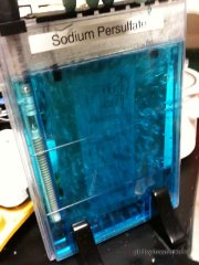
Bubbles decrease the reaction time by wicking away solution that has already reacted. As soon as both sides are dissolved, remove it from the solution and rinse with water.
Finishing
Put the solution back in the original container. It can not be thrown down the drain since it’s a biohazard. To finish the board, all you have to do is connect both sides electrically. To do this quickly, take very fine wire and strip it. Sew the wire through every hole on your board. Solder both sides of the wire in place using as little solder as possible. Then clip the wire as close as possible using wire cutters. Finally, add a bit of flux to each spot and touch it up with the iron. This will smooth out the via.
