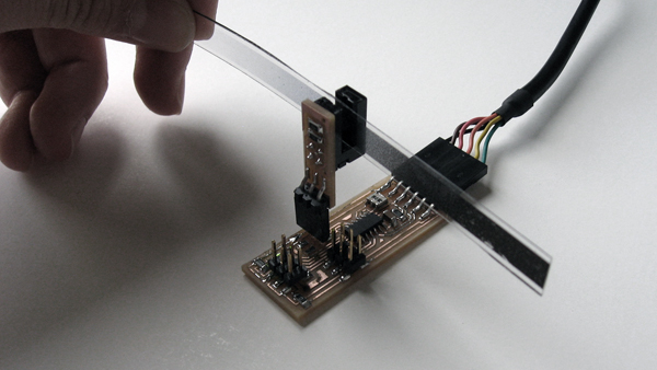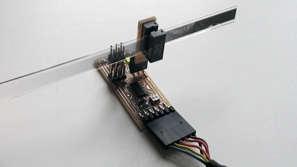
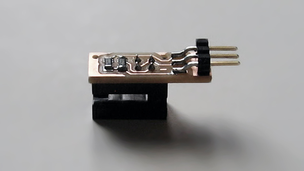
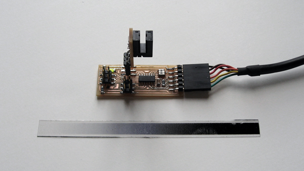
For my final project I need to sense linear position and thus I decided to try out an Optical Interrupter. I used the TCST5250 but for next iteration I want to try the EE-SX1108 which is smaller and SM.
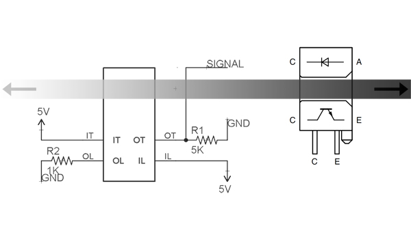
This sensor is basically an LED and a Phototransistor that work together to produce an analog signal according to the transparency of the material placed between them. I printed out a gradient in a transparency strip which is placed in the sensor's slot between the LED and the Phototransistor. By moving this strip linearly the sensor produces a variable DC level. What is interesting, is that this strip is a sort of a ‘program’: it is possible to produce different behaviors (linear or-non-linear) according to what is printed on the strip.
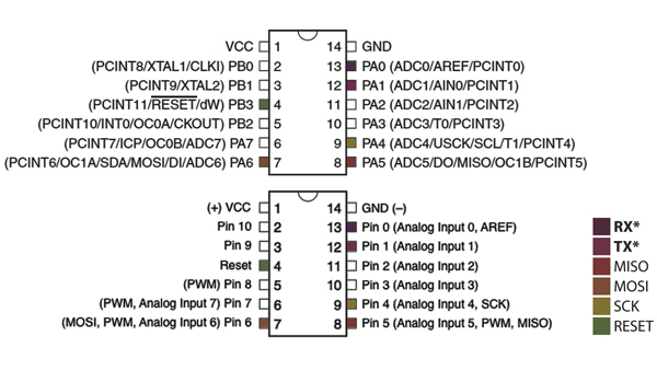
The ATtinny44 is a low-power CMOS 8-bit microcontroller with two Ports (A and B) based on the AVR enhanced RISC Architecture . The two layouts above show the Ports on the ATtinny44 and their correspondence for the Arduino Environment. For more details refer to Devid Mellis’ tutorial.
PORT A is a 8-bit (PA0 to PA7) bi-directional I/O port with internal pull-up resistors. Port A has alternate functions as analog inputs for the ADC, analog comparator, timer/counter, SPI (Serial Peripheral Interface) and pin change interrupt.
Port A, Bit 0 (PA0/Pin 0):
ADC0: Analog to Digital Converter, Channel 0.
AREF: External Analog Reference for ADC. Pullup and output driver are disabled on PA0 when the pin is used as an external reference or Internal Voltage Reference with external capacitor at the AREF pin by setting (one) the bit REFS0 in the ADC Multiplexer Selection Register (ADMUX).
PCINT0: Pin Change Interrupt source 0. The PA0 pin can serve as an external interrupt source for pin change interrupt 0.
Port A, Bit 1 (PA1/Pin 1):
ADC1: Analog to Digital Converter, Channel 1.
AIN0: Analog Comparator Positive Input. Configure the port pin as input with the internal pullup switched off to avoid the digital port function from interfering with the function of the Analog Comparator.
PCINT1: Pin Change Interrupt source 1. The PA1 pin can serve as an external interrupt source for pin change interrupt 0.
Port A, Bit 2 (PA2/Pin 2):
ADC2: Analog to Digital Converter, Channel 2.
AIN1: Analog Comparator Negative Input. Configure the port pin as input with the internal pull-up switched off to avoid the digital port function from interfering with the function of the Analog Comparator.
PCINT2: Pin Change Interrupt source 2. The PA2 pin can serve as an external interrupt source for pin change interrupt 0.
Port A, Bit 3 (PA3/Pin 3):
ADC3: Analog to Digital Converter, Channel 3.
T0: Timer/Counter0 counter source.
PCINT3: Pin Change Interrupt source 3. The PA3 pin can serve as an external interrupt source for pin change interrupt 0.
Port A, Bit 4 (PA4/Pin 4):
ADC4: Analog to Digital Converter, Channel 4.
USCK: Three-wire mode Universal Serial Interface Clock.
SCL: Two-wire mode Serial Clock for USI Two-wire mode.
T1: Timer/Counter1 counter source.
PCINT4: Pin Change Interrupt source 4. The PA4 pin can serve as an external interrupt source for pin change interrupt 0.
Port A, Bit 5 (PA5/Pin 5):
ADC5: Analog to Digital Converter, Channel 5.
DO: Data Output in USI Three-wire mode. Data output (DO) overrides PORTA5 value and it is driven to the port when the data direction bit DDA5 is set (one). However the PORTA5 bit still controls the pullup, enabling pullup if direction is input and PORTA5 is set (one).
MISO: Master Data input, Slave Data output pin for SPI channel. When the SPI is enabled as a Master, this pin is configured as an input regardless of the setting of DDA5. When the SPI is enabled as a Slave, the data direction of this pin is controlled by DDA5. When the pin is forced by the SPI to be an input, the pull-up can still be controlled by the PORTA5 bit.
OC1B: Output Compare Match output: The PA5 pin can serve as an external output for the Timer/Counter1 Compare Match B. The PA5 pin has to be configured as an output (DDA5 set (one)) to serve this function. The OC1B pin is also the output pin for the PWM mode timer function.
PCINT5: Pin Change Interrupt source 5. The PA5 pin can serve as an external interrupt source for pin change interrupt 0.
Port A, Bit 6 (PA6/Pin 6):
ADC6: Analog to Digital Converter, Channel 6.
SDA: Two-wire mode Serial Interface Data.
DI: Data Input in USI Three-wire mode. USI Three-wire mode does not override normal port functions, so pin must be configure as an input for DI function.
MOSI: Master Data output, Slave Data input for SPI channel. When the SPI is enabled as a Slave, this pin is configured as an input regardless of the setting of DDA6. When the SPI is enabled as a Master, the data direction of this pin is controlled by DDA6. When the pin is forced by the SPI to be an input, the pull-up can still be controlled by the PORTA6 bit.
OC1A, Output Compare Match output: The PA6 pin can serve as an external output for the Timer/Counter1 Compare Match A. The pin has to be configured as an output (DDA6 set (one)) to serve this function. This is also the output pin for the PWM mode timer function.
PCINT6: Pin Change Interrupt source 6. The PA6 pin can serve as an external interrupt source for pin change interrupt 0.
Port A, Bit 7 (PA6/Pin 7):
ADC7: Analog to Digital Converter, Channel 7.
OC0B, Output Compare Match output: The PA7 pin can serve as an external output for the Timer/Counter0 Compare Match B. The pin has to be configured as an output (DDA7 set (one)) to serve this function. This is also the output pin for the PWM mode timer function.
ICP1, Input Capture Pin: The PA7 pin can act as an Input Capture Pin for Timer/Counter1.
PCINT7: Pin Change Interrupt source 7. The PA7 pin can serve as an external interrupt source for pin change interrupt 0.

PORT B is a 4-bit (PB0 to PB3) bi-directional I/O port with internal pull-up resistors.
Port B, Bit 0 (PB0/Pin 10):
XTAL1: Chip Clock Oscillator pin 1. Used for all chip clock sources except internal calibrateble RC oscillator. When used as a clock pin, the pin cannot be used as an I/O pin. When using internal calibratable RC Oscillator as a chip clock source, PB0 serves as an ordinary I/O pin.
PCINT8: Pin Change Interrupt source 8. The PB0 pin can serve as an external interrupt source for pin change interrupt 1.
CLKI: Clock Input from an external clock source.
Port B, Bit 1 (PB1/Pin 9):
XTAL2: Chip Clock Oscillator pin 2. Used as clock pin for all chip clock sources except internal calibrateble RC Oscillator and external clock. When used as a clock pin, the pin cannot be used as an I/O pin. When using internal calibratable RC Oscillator or External clock as a Chip clock sources, PB1 serves as an ordinary I/O pin.
PCINT9: Pin Change Interrupt source 9. The PB1 pin can serve as an external interrupt source for pin change interrupt 1.
Port B, Bit 2 (PB2/Pin 8):
INT0: External Interrupt Request 0.
OC0A: Output Compare Match output: The PB2 pin can serve as an external output for the Timer/Counter0 Compare Match A. The PB2 pin has to be configured as an output (DDB2 set (one)) to serve this function. The OC0A pin is also the output pin for the PWM mode timer function.
CKOUT - System Clock Output: The system clock can be output on the PB2 pin. The system clock will be output if the CKOUT Fuse is programmed, regardless of the PORTB2 and DDB2 settings. It will also be output during reset.
PCINT10: Pin Change Interrupt source 10. The PB2 pin can serve as an external interrupt source for pin change interrupt 1.
Port B, Bit 3 (PB3/Reset):
RESET: External Reset input is active low and enabled by unprogramming (“1”) the RSTDISBL Fuse. Pullup is activated and output driver and digital input are deactivated when the pin is used as the RESET pin.
dW: When the debugWIRE Enable (DWEN) Fuse is programmed and Lock bits are unprogrammed, the debugWIRE system within the target device is activated. The RESET port pin is configured as a wire-AND (open-drain) bi-directional I/O pin with pull-up enabled and becomes the communication gateway between target and emulator.
PCINT11: Pin Change Interrupt source 11. The PB3 pin can serve as an external interrupt source for pin change interrupt 1.
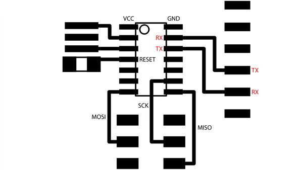
PORTS SUMMARY(for Board Layout):
RX: Recieve Data on PA0/Pin 0 (*goes to TX in FTDI cable).
TX: Transmit Data from PA1/Pin 1 (*goes to RX in FTDI cable).
Serial Peripheral Interface (SPI): Synchronous serial data protocol used by microcontrollers for communicating with one or more peripheral devices quickly over short distances. It can also be used for communication between two microcontrollers. With an SPI connection there is always one master device (usually a microcontroller) which controls the peripheral devices. Typically there are three lines common to all the devices:
MISO (Master In Slave Out): Slave line for sending data to the Master.
MOSI (Master Out Slave In): Master line for sending data to the Slave.
SCK: Clock pulses to synchronize data transmission generated by the master.
RESET: External active low signal resets the microcontroller.
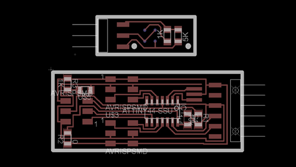
Eagle files for the Sensor and FaBread Schematic and Board Layout.
Library file with the Optical-Interrupter and three and five pin connectors.
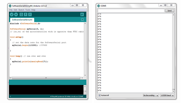
//before starting: Tools=>Board=>ATtinny44
#include SoftwareSerial.h
SoftwareSerial mySerial(0, 1); // (rx,tx) on ATtinny44
void setup()
{
mySerial.begin(115200); // change BAUD in Serial Monitor
}
void loop() // run over and over
{
mySerial.println(analogRead(7)); // ADC pin on ATtinny44
}