Week Ten: Output Devices
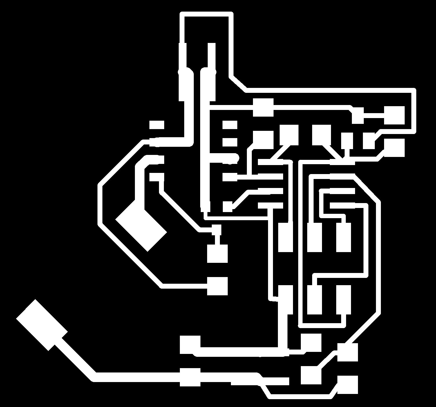
This week we were making output devices! I decided to hijack it to do some testing for my final project, so I made a buck converter. My final project involves a controllable constant current output into a wire for hot-wire cutting. The final version will use the 16A mosfets in the lab, but since there wasn't a corresponding p-type mosfet, I went with just using an h-bridge to do my testing with. I mostly wanted to check out how difficult it would be to use the built-in PWM mechanisms and dead-time generators on the ATtinys. Since I wanted a relatively high current, I opted to use the 10 microH inductor, which is rated for 3.9A (the 1.2 microH inductor would require me to switch at ~MHz). I calculated that with the 10 microH inductor, I'd need to switch at 200kHz. I decided to use a 10 microF capacitor because that'd give me ~16 kHz oscillator frequency and the bode plot said the gain wasn't too scary there. Here's the final board I made:

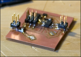
I actually made two boards that I stuffed. I discovered that the first one I made (pictured below) would probably have let out magic smoke if I tried to program it: I used OC1A and -OC1A as my PWM and -PWM, but they're also the pins for MISO and MOSI. I looked up the timing diagrams on the data sheet and it seemed like those would go on at the same time, thus causing shoot-through in my mosfet totem... so I didn't try programming it, and redesigned the board.

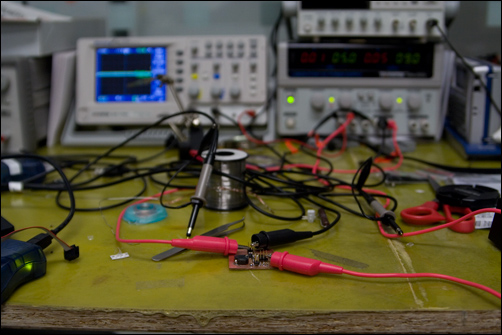
Made the second board, stuffed it, etc. I think my first attempt at it had a short somewhere, so I desoldered it (a few times) looking for it. The second time I desoldered it was when I saw 41.6kOhms between my 5V and ground, but I eventually figured out that that was an acceptable resistance when I measured just one of the 5V regulators not on the board. Then I ran into problems because my pull-up resistor on the n-fet driving the p-fet was too large and not charging the p-fet gate fast enough, so I was getting shoot-through. I ended up stacking 3 499ohm resistors on top of each other to reduce that resistance without going out of the resistor's wattage rating. Then I got a fairly acceptable pwm signal (yellow is p-fet gate, blue is n-fet gate):


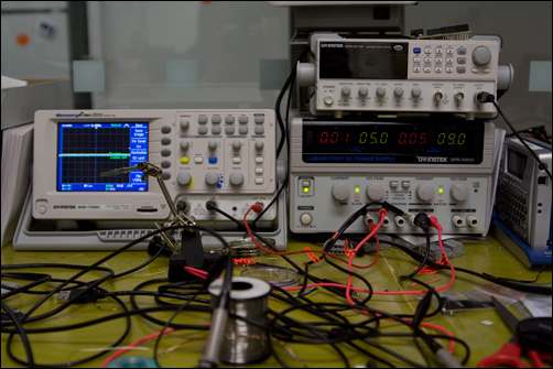
And it bucks fine! I had about a 60% duty cycle going, and got around 4.3V at 7V input, and 6V at 9V input. There was a bit of voltage ripple (about 1V p-p), so I might stick a bigger cap on there. Here's the output traces of those two:
I tried doing feedback on the output voltage, but I think I need to actually design the control system for that so it can be really good. Right now the voltage is feeding into the one last ADC I have left, so I might switch to an attiny with more pins so I can have a pot comparing to that voltage output and regulating that way. Anyway, when I tried to do feedback, I once got a perfect square wave (so my gain of 1 was probably too high), and other times got other values that I found difficult to diagnose... so I decided to work on that another time.
Oh, and here's my code! Done in assembly :)
.include "tn45def.inc"

.def temp = R16; temporary storage
.def temp1 = R17; temporary storage
.def ah = r19; adch
.def al = r20; adcl

.org 0
rjmp reset

;
; main
;
reset:
	;
	; set fuse low byte to 0x7E for 20 MHz resonator
	;
	; set clock divider to /1
	;
	ldi temp, (1 << CLKPCE)
	ldi temp1, (0 << CLKPS3) | (0 << CLKPS2) | (0 << CLKPS1) | (0 << CLKPS0)
	out CLKPR, temp
	out CLKPR, temp1

	;
	; set stack pointer to top of RAM
	;
	ldi temp, high(RAMEND)
	out SPH, temp
	ldi temp, low(RAMEND)
	out SPL, temp

	;
	; start main loop
	;
	sbi DDRB, 3
	sbi DDRB, 4
	ldi temp, 0b11010001
	out TCCR1, temp
	ldi temp, 0b01010000
	out GTCCR, temp
	ldi temp, 0b00101000
	out OCR1C, temp
	lsr temp
	out OCR1B, temp
	ldi temp, 0b00000010
	out DTPS1, temp
	ldi temp, 0b00100100
	out DT1B, temp
	clc

	cbi DDRB, 2
	cbi PORTB, 2

	loop:
		rjmp loop