week three: in-system programmer
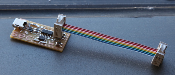
This week, we were charged with building an in-system programmer, a device that will translate programs from a computer to other microcontroller chips. Starting with a cut file for the traces, we etched PCB stock using the Modela mill with a 1/64" bit. After cutting out the board with the 1/32" bit, we stuffed and soldered the board. Finally, we programmed the programmer using avrdude.
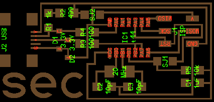
I started from Neil's Hello-ISP.cad design, adding my initials using Matt's new text module for kokopelli. I am building from source, but I believe this library is available in the newest package. This took very little new work -- the new code is shown below. First we import the text module, then we create a subclass of part for adding text to the trace layer. Finally, we create an instance with my initials and add it to the board.
import koko.lib.text as kt


class initials(part):
   #
   # sign your initials
   #
   def __init__(self,name='',h=.1,rot=0,offset=[0,0]):
      self.value = ''
      self.pad = []
      self.labels = []
      self.shape = rotate(kt.text(name,offset[0],offset[1],h,'LB').s,rot)

L1 = initials('sec',.37,-90,[.02,.03])
pcb = L1.add(pcb,x,y+height,z)
It took me two tries to mill the board correctly -- The first time I exported a PNG of 'exterior' and used the fab modules to cut out the board. Although the geometry is exactly the same as 'interior', the orientation is flipped (white and black are switched). As a result, the fab modules offset by half the kerf in the wrong direction, making a cut that was one kerf width too small. As a result, the outer traces were cut off. After realizing what I had done wrong, this was an easy mistake to fix.
To clean the board, I followed Nadya's recommendation, using Gojo abrasive hand cleaner to get rid of the copper spider webs. I think it worked best using just my thumb -- I tried with a brillo pad, but this actually started to peel back one of my traces.
 |
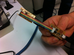 |
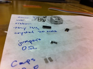
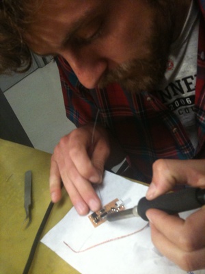
Above are some pictures from the stuffing and soldering process. On the left, taping and labeling all parts was incredibly helpful to keep track of parts smaller than a grain of rice. On the right, my board is programmed by Dan's board using avrdude. While soldering, Noah and I found that the pad for SJ1 (one of the jumpers) wasn't quite the right shape. Here is a code fix (line 3630) to make the pads better fit the jumper:
#SJ1 = SJ('SJ1')
SJ1 = R_1206('SJ1')
pcb = SJ1.add(pcb,IC1.pad[7].x-.07,J1.pad[5].y,z,angle=90)
Also, thanks to Sujoy for grabbing a picture of me in action:
Files: