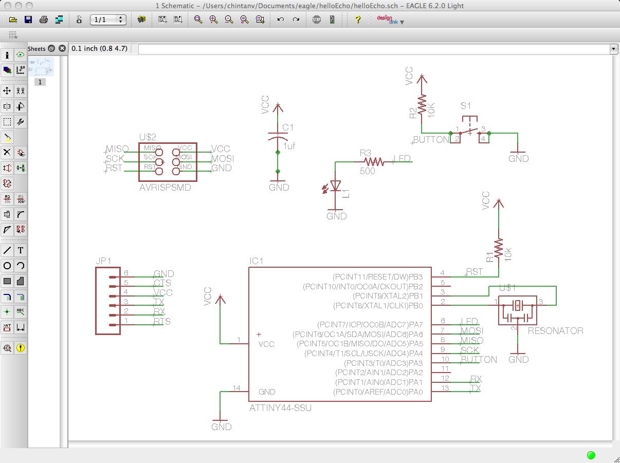
Schematic (Front)
To design a circuit board with micro-controller that operates an LED with the help of a button.
The schematic design was straight forward with the help of the tutorial in fab academy.
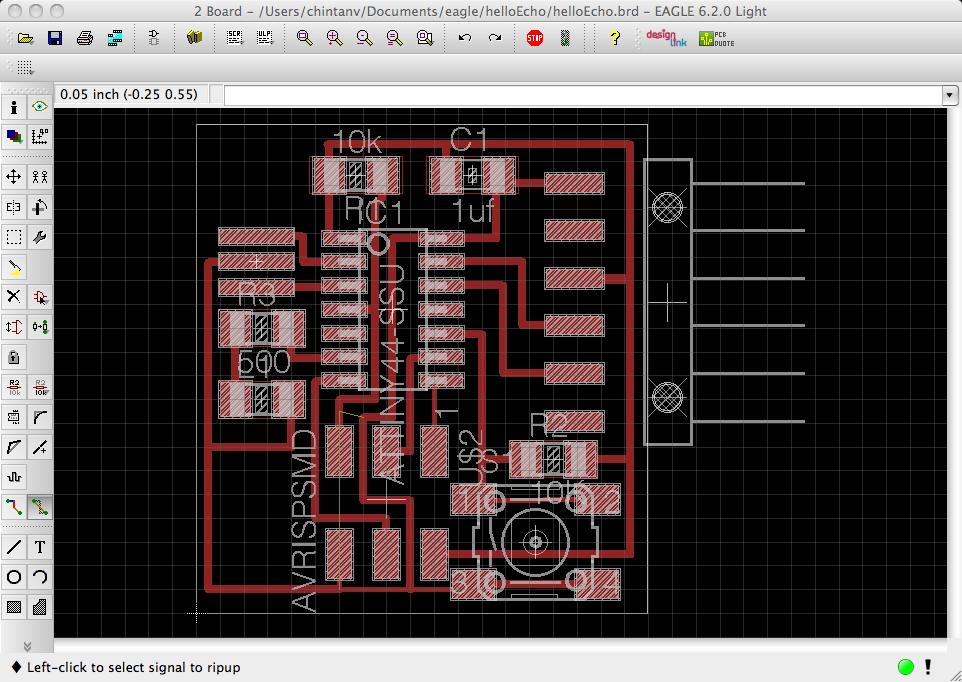
The board design was challenging and tedious. It was very hard to overcome crossover points even after trying all the tricks. Ultimately, a combination of rearranging the components and autorouting traces with routing grid set to 10 mil worked well. Auto routing got about 75% of traces routed. The final three or four that needed routing were super tricky as well.
I tried the following tricks:
Upon running DCR, Eagle complained about several errors (18 in total) about clearnances being small. I adjusted tracks using ALT+Move, and got it down to 11. At this point, the clearances looked reasonably good, and I decided to go ahead with milling the board. In all, editing the board took several hours of iterations before I had a board that was satisfactory.
The following two Eagle tutorials were very helpful:
Eagle Tutorial 1 by Jeremy Blum
Eagle Tutorial 2 by Jeremy Blum
Exporting the board (traces and outer edges) using Eagle and GIMP was easy. An important step here was to invert the images (using "image->invert" on GIMP) so that copper to be removed from the board is in white.
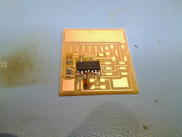
I had to mill the board on Modela twice. First time around, the 1/64 drill bit must have gotten pushed up as I tightened the screws. Consequently, the traces came out light. Next time, I adjusted the drill bit, but also deepened the z-axis of the path to -0.15 (instead of -0.1). The board came out perfectly.
I faced two challenges whil stuffing the board:
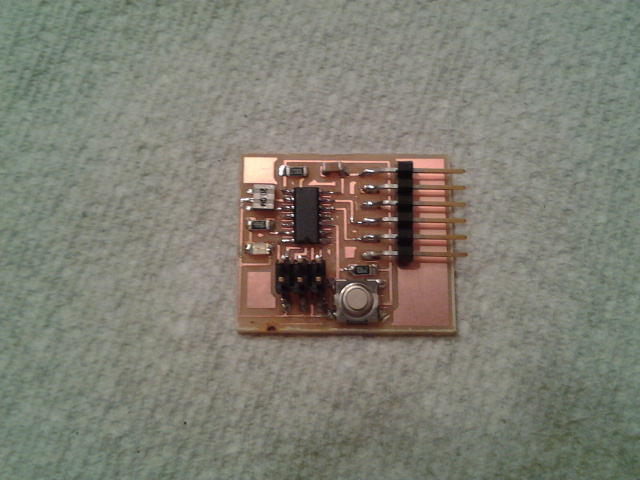
Hopefully, the board will work next week.