ELECTRONICS DESIGN
Elaborating on what the class learned in making the FabISP, this week the assignment took
the process one step further: we learned to design our own PCBs using EAGLE
(Easily Applicable Graphical Layout Editor) PCB Design Software. The assignment was to redraw and make the
echo hello-world
board and add (at least) a button and an LED (and current-limiting resistors).
After drawing in all the wires in the schematic using the "wire" command, I read a couple of
Eagle tutorials online and discovered the "net" tool that automatically couples wires together
(after asking you, of course :) ). Instead of using an actual line on the screen to link two
components together, you can draw two short segments of wire (using the "net" command) from the
appropriate pins of the two (or more) separate components. Right-click on the component or
use the command "name" to select one of the wire segments. For example, you can name the first
wire (coming from pin 10 of the ATTINY-44) "BUTTON", and name the wire at the other end "BUTTON"
as well. The program will ask you: "Connect N$[#] and BUTTON?" Click yes to connect and
associate the two+ pieces. In "Board" view, the two components will appear to be connected by
a thin line. Right-click the line to route traces between components drawn to scale.
I forgot to do a DRC (Design Rules Check) and an ERC (Electrical Rule Check) before exporting my
board as a PNG. After already having recreated my PNG once to try and correct the error, the DRC
caught one major error: not enough clearance between the lower left pad of the 2x3 header
and the trace passing by right above it. The DRC did not catch errors I found only after
milling the board. Three more traces (all in the central region of the PCB) were too close
to their neighboring pads. When the fab modules created the 4 tool paths to mill the board,
the paths did not run between these traces and pads. In the actual "finished" board, the
traces and pads are stuck together. Despite trying my best to use the X-ACTO knife to separate
the traces and the pads, I keep discovering more of these conditions so I will have to recreate
the board and mill a third time.

One other design tool I did not discover until late in the PCB fabrication process is that you
can change the grid size. I had been manually adjusting the positions of each wire in the
Properties menu, but hopefully, in the newest redesign, the change of grid size from 0.05 to
0.025 inches will help to resolve the conditions from the previous two PCB iterations.
I could have saved myself some trouble if I had just used the vinyl cutter like I had originally
planned. Using the Default settings in the fab modules, the tool path generated did not run
into any of the issues I had with the milling process.


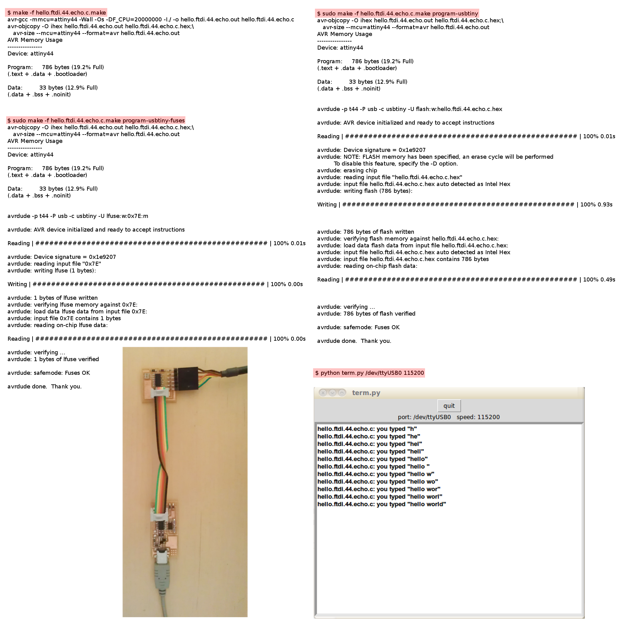
I started attempting to program the echo hello-world board using the Programming
tutorial. I got stuck on this step:
$ sudo make -f hello.ftdi.44.echo.c.make program-usbtiny-fuses
Following TA Matt's helpful debugging tips for the FabISP
and without realizing the errors in my own board, I came to the conclusion that the FabISP
that I had borrowed did not work for some reason or another. With the appropriate drivers
installed on your operating system (for Mac OS X - CrossPack for AVR Development),
typing in:
avrdude -c usbtiny -p t44
should prompt the response
avrdude: initialization failed, rc=-1
Double check connections and try again, or use -F to override
this check.
***avrdude: error: usbtiny_transmit: usb_control_msg(DeviceRequestTO): unknown error***
avrdude done. Thank you.
The part inside the *** *** seemed to suggest that there was something wrong with the
FabISP itself. In a couple of days, I will try this out again, and I hope to succeed
next time :D.
Looking ahead to the Final Project, some thoughts
from DigiKey. IR LEDs and phototransistors!!