2012 How to Make almost Anything
The first step is to mill out the traces out of copper. The copper gives a great surface for the solder to stick to, and it is non toxic so it is safe to mill. The png file used can be found here.

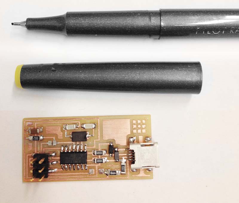
After the piece has been removed and is securely placed on the table the soldering can begin. It is important to organize where all of the pieces are going first. The location of all of the components can be seen here. Mapping out the order that you are to solder in is important since the board is so tiny. It is almost impossible to work around a poorly planned board.

Here is the final piece with all of the components soldered into place. It is important to affix only the necessary amount of solder to the board, because any extra mess could short out one of the components. This image does not have the two jumpers soldered in place which is necessary for programming.

The final step is to connect your board via USB to the computer and with the correct firmware installed begin programming your board. The programmer used is AVR and it connects directly to the 6 prongs on top of your board and into the computer. The Technical aspect is foreign to me but a good tutorial on how to program the board can be found here.
My board was in perfect shape so that when I programmed the board I recieved no errors. I was extremely fortunate. This just solidifies how important the method that you use to solder is, in respect to the sucess of your finished FabISP.
Once the program is installed the two jumpers can be removed in order for the ISP to program additional boards.