2012 How to Make almost Anything
FINAL BOARD DESIGN

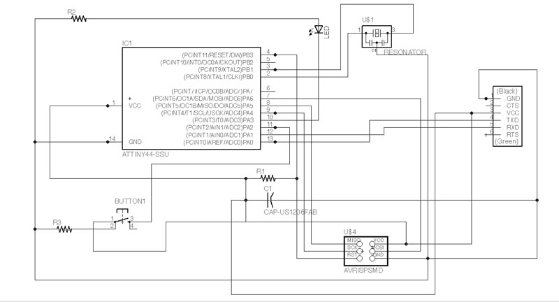
The most important step in this process is the layout of a clean electrical schematic. As you can see from this early image, the difference between joints, overlaps and connections is not very clear. The placement of the parts in the schematic design is as important as the Board layout. Try and position parts so that they create layered routing lines rather than crossed. Also use the add joint button in eagle to distinguish between common overlaps and physical joints. A messy schematic will lead to increased confusion when trying to neatly organize your final board layout.
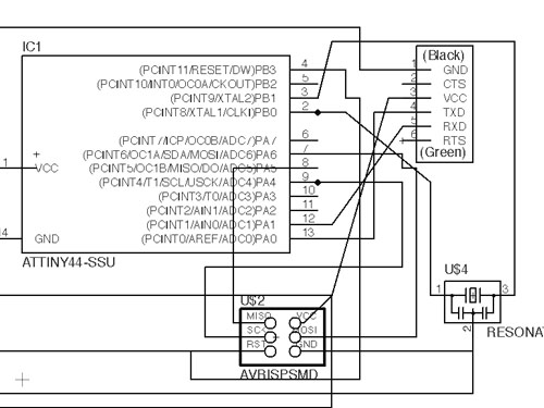
Eagle has a useful feature that allows you to create board layouts directly from schematic relationships. This image is the "auto route" feature of Eagle. It was very quick in decideing where all of the routes were to go. It however was not practical to mill out.
You can also manually route the wires by hand, by clicking the lines that connect parts togehter from the schematic and snaking the routes around. I am not very satisfied with this process, the controls did not let me experiment with different configurations in a quick manner, and the grid that the lines snapped to felt very limiting. More time spent with it would yield better results, but I decided to move on to illustrator to route the paths and produce the png.
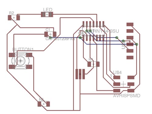
In illustrator it was important to get the right size for the pads and lines. I imported this file, and traced the common pad sizes and grouped them by component. The path tool was used to create the lines. I initially had a thickness of 1pt, but that proved to be too thin. 1.3pt seemed to be the minimum stroke weight i would use.
Layer management is extremelely important. make sure you have each components pads, in a separate layer so you can easily identify the placement of each. This will also assist in making this process somewhat parametric. stroke width can be used to chnage multiple pads at once.

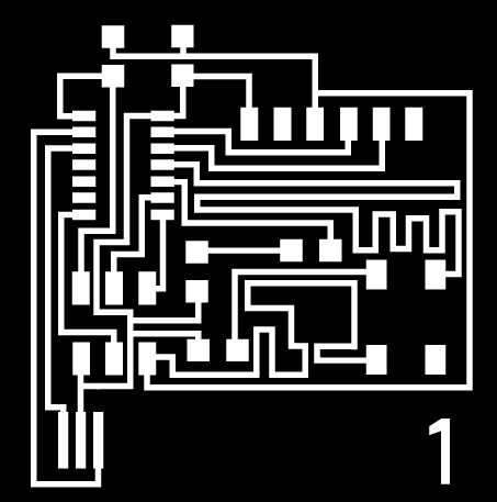
Here is the Modela Milling out my designed board
Milling the board is a prcess that I covered in week 3. visit this page for more info. This also contains info on soldering.
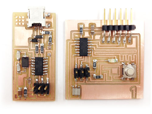
My final is board is about twice as large as the original programmer. Even with about half as many components this board has a much more complex wire arrangement. My inexpereince in routing the board efficiently also led to this increase in size.
The square shape is a good fit in the hand for the ability to press the button.
Programming the board will be the final say on whether it is a sucessful deisgn and build.