Rotem Abeles - How to make (almost) everything – Fall 2013
WEEK 6 – PCB design
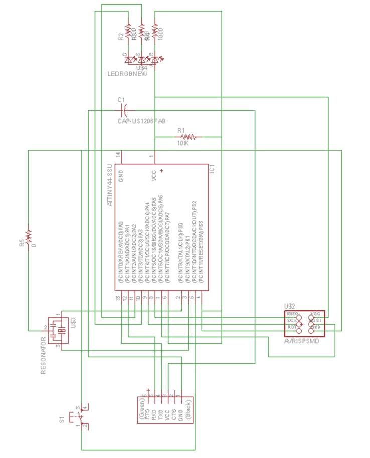
This week’s task was to redesign the Hello_fab board and add a switch and LED to it.
I was using Eagle for designing the board, and it took some time and guidance to get used to it. I attended Raj’s intro session on Friday and followed this tutorial on fabacademy.
The biggest problem I had was that lines in the schematic view did not appear in the board view. Raj explained to me that it was because I didn’t connect lines exactly to the ends of the component. Unlike many apps I used to, lines\connectors in Eagle are not “magnetic”, meaning they don’t have any tolerance for even the slightest misplacement.
I used the RGB LED instead of the 1206 LED to be able in the next week to program a rainbow J
0 ohm resistor to act as a bridge over an unavoidable
trace Each LED color gets its own resistor and is connected to
a separate leg on the microcontroller![]()
![]()
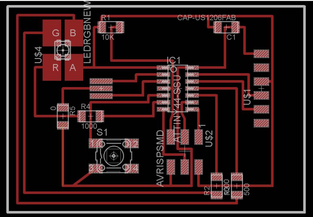
In the board design view I used DRC extensively (with 10mil setting) until I got the clearances right. I purposely designed a bigger board than I needed to make soldering easier.
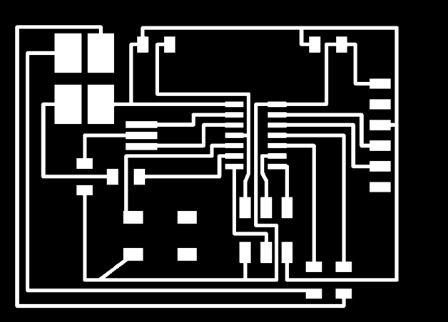
And the PNG export (top traces only, monochrome, 500dpi):
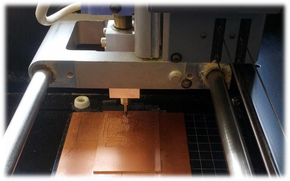
When I got to the modela (actually, to the make .rml process) I found some critical technical mistakes:
1. I wanted to insert my initials on the board. For this, I added the text to the PNG using painter. When I got to the fab modules I realized it messed up with the resolution.
2. I didn’t change the canvas size of the board in Eagle. That created a too big of a PNG which I had to crop using a photo editing tool. It was actually easier to go back to eagle and adjust the board border and then export the PNG again.
3. As a consequence of the last item, my cutout had to be resized. Vivek helped me use the fab modules itself to do that, by writing down the x,y dimensions of the traces PNG.
Milling went smoothly using Z depth of -0.13 for the 1/64 end mill and -0.6 for the 1/32 end mill.
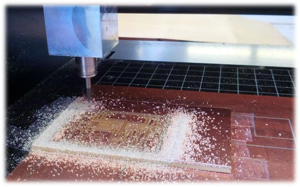
Traces cutout
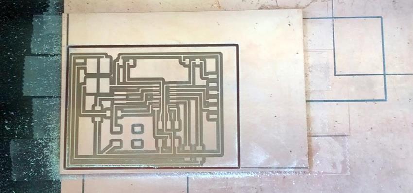
Board completed [Note the marks of the erroneous cutout]
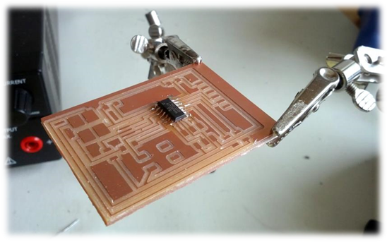
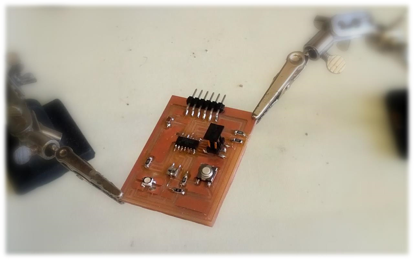
After setting all the components I need on paper using double sides scotch, I started soldering. Although 15 years passed since that last time I was soldering, I quickly got the hang of it. Neil’s illustrations from week 2 were very useful as soldering best practices, and I was trying to mimic those guys from Neil’s description of soldering masters that make it look easy.
 =>
=> =>
=>
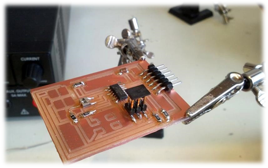
Complete board:
And now, programming...