 |
||||||||||||
| HOW TO MAKE (ALMOST) ANYTHING MIT MEDIA LAB |
|
PROJECTS | ABOUT | CONTACT | ||||||||
|
|
|||||||||||
| ISP IN-CIRCUIT PROGRAMMER - week3 | ||||||||||||
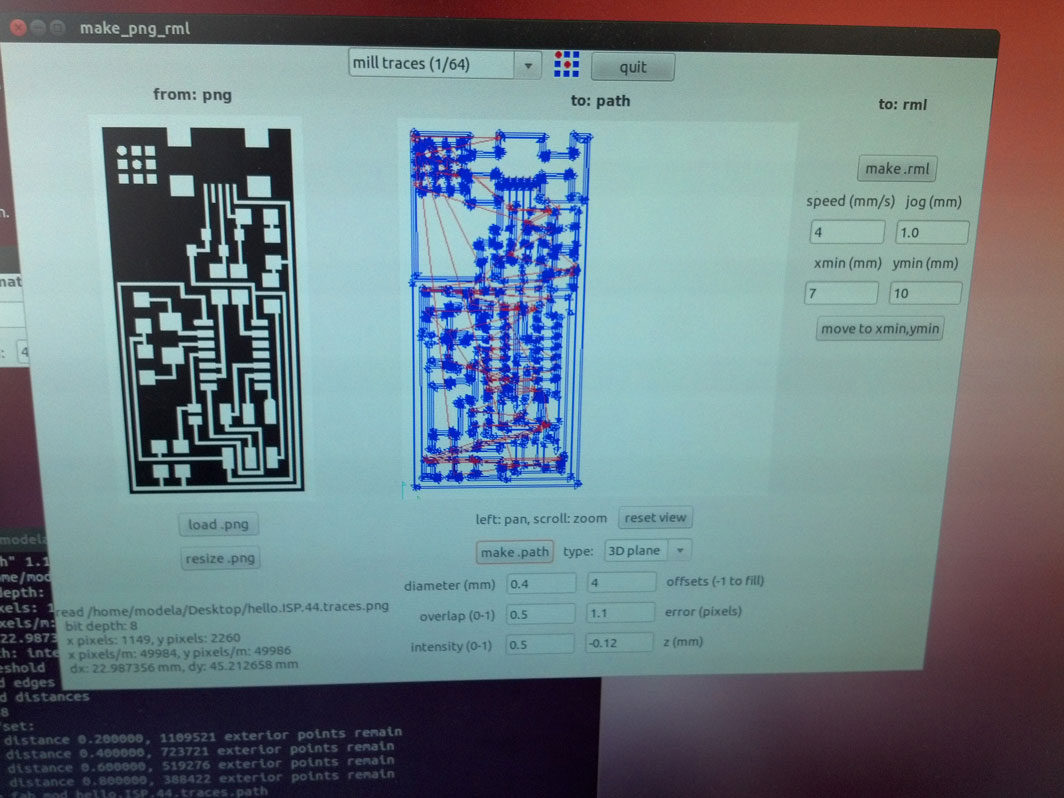
I learned this week that in electronics there lies a good deal of magic. The first step was to use the milling machine to make the board. I used the hello.ISP.44.cad to mill the trace and the interior. The initial settings, guided by the presets in the Fab Modules seemed to work: .Milling the trace with 1/64 tip, 4 offsets, 0.4 diameter, -0.13 depth .Milling the interior with 1/32 tip, cut depth at 0.6, and offset set to 1 It was, in fact, exciting to use the Fab Modules properly this week as I didn't play with them that much last week. |
||||||||||||
 |
||||||||||||
| the fab modules - making path and adjusting parameters for the Modela milling machine | ||||||||||||
 |
||||||||||||
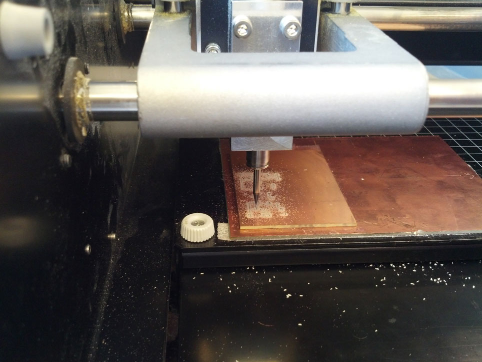
| Modela working out | ||||||||||||
 |
||||||||||||
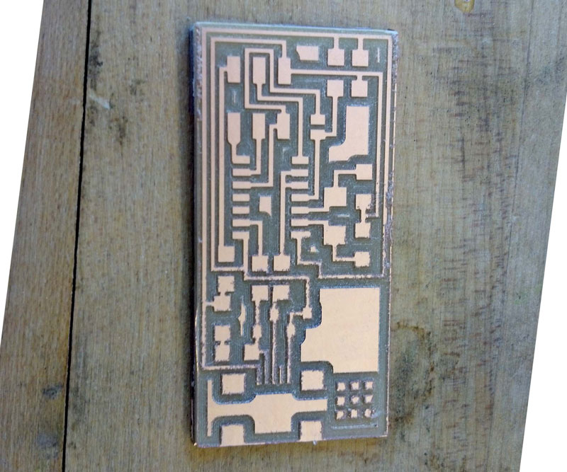
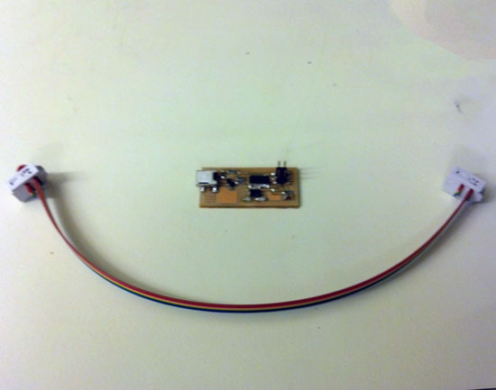
| board cut out! Some edges less defined, but no grave problems | ||||||||||||
| Problems | ||||||||||||
| The view option on the machine was useful for adjusting xmin,ymin, pausing in case of problems as well as adjusting length of the drilling tip. But the most useful thing to remember was to write down the parameters of xmin, ymin. My software froze and I had to restart the machine, and if I hadn't written down where the x,y origin was that I set it to, I would have had to restart the milling as well as these traces are too detailed to "eyeball" a second trace. As you can see from the photo above, not all the edges were nice and straight. It likely had to do with the double sided tape underneath being a little bit uneven. To make sure that the board is still functional though, I used a voltmeter to detect whether or not there was current flow between two distance points connected by some segment too thin. All was good so I went on with the next part. | ||||||||||||
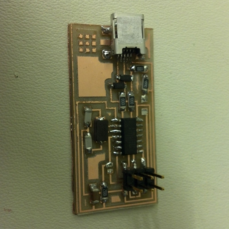
| Step 2 - Soldering | ||||||||||||
| The soldering was actually not so bad, particularly when I discovered the super useful copper ribbon to take away excessive solder. The trick to just dump a lot of solder on the really fine legs and then soak it up with the ribbon worked really well. First time around, however, something still didn't work, but going over the various parts adding a bit more solder where there might be gaps did the trick. | ||||||||||||
 |
||||||||||||
| Step 3 - Programming | ||||||||||||
| Now this bit was magic. These were the instructions, which I followed with the lab guru's help: USB power make clean make hex (sudo) make fuse (check programmer in Makefile, may need to repeat) (sudo) make program desolder SJ1 and SJ2 make IDC ISP cable, connecting header pin 1 to pin 1 Apparently now this ISP is ready to be used as a programming device, am looking forward to learning more about how! | ||||||||||||
 |
||||||||||||
| Copyright 2013 by Anya Yermakova | ||||||||||||