
This week we need to program our boards designed in week 5 in as many languages possible and to do as many things possible. Our boards should attempt to take over the world. And embedded programming sounds so cool. Everything sounds more impressive if you add the word embedded in front of it. Spies were embedded deep in the heart of the operation. Donuts embedded in chocolate glaze are her downfall. He is a thorn embedded in her side. Embedded programming is for superheroes. Cuteness embedded within a document will distract you from my half finished assignment. See, embeddedness takes things up a notch!

I didn't get a chance to finish the assignment for week 5 so I spent a huge portion of this week finishing. I read a lot of past year's webpages and some common mistakes were having the LED facing the wrong direction, and failing to add the unnecessary pull up resistor. I added a new pull up resistor and rerouted the board, first I used autoroute and then I manually ripped up a lot of the connections and routed the connections by hand. I really wanted to learn to vinyl cut the circuit so I struggled to keep everything on one layer with no vias or intersections. I looked at other layouts for guidance. Originally everything was placed at right angles but I read online that this was bad for flexible circuits so I tried to minimize the right angles. My 2 year old sat on my lap while I rerouted the circuit and moved everything around and he called the circuit a robot and wanted to know where the robot was going.
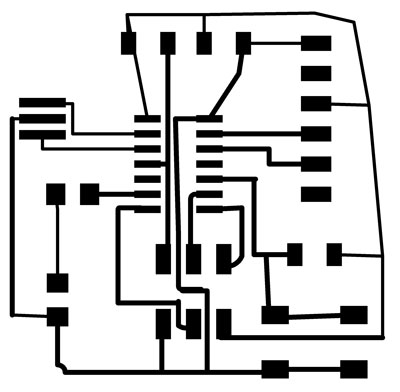
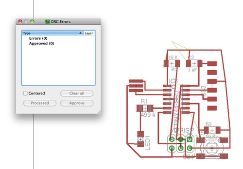
Finally no errors when doing design rule check. Rerouting this board and figuring out where to place components took over 5 hours! Am I doing something wrong here? Also am using the wrong ISP header pads. So switched to schematic view and used the replace part command to choose the correct header.
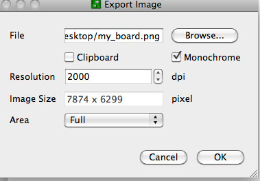
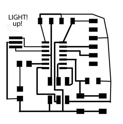
In eagle, select the layer you want to display, select export, select monochrome, set dpi to 2000 and save image.
Opened image in photoshop to create board outline and to add lettering to the board

I really want to learn to make a flexible circuit for my final project. Figure this is a good week to do it. For this week I want to mount my vinyl cut circuit on a piece of glass and create a stained glass circuit where the circuit is mounted onto the top of a little box. I followed the steps on the tutorial here:
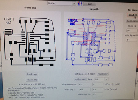
http://fab.cba.mit.edu/content/processes/PCB/vinylcut.htmlAnytime the vinyl cutter wasn't working I restarted the machine and restarted the fab modules and tried again. First started in windows but the Corel Draw license was expired so rebooted into Linux and used the fab modules and they worked swimmingly. A few minor quirks. The tutorial said to resize your png to match the copper piece you are using this will actually resize your entire png so you will get a huge circuit if you have the keep proportions button checked. It took awhile to get the machine working but when it did it cut the circuit Way too fast and tore up all of the traces. So I adjusted my cutting speed and pen force and tried again. I tried multiple settings until I got the one that was just right!
Then placed masking tape over the circuit and lifted it off and it came up easily.
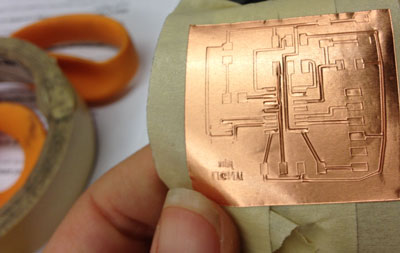
Transferred the circuit to my glass substrate and while the masking tape was still on I rubbed the masking tape with the side of a pair of scissors so it would stick to the glass. Then I lifted the masking tape off and the copper stayed on the board.
Weeded out the excess copper this was painstaking and accidentally cut traces several times when doing this so repeated the process 3 times. Charles (our amazing lab manager) said that my cuts weren't all of the way through which is why it was so difficult to weed. So tried even more settings. The problem was if it cut all the way through the pen would then drag and rip up the precut traces. The path needed to go from interior to exterior to avoid this hapening?
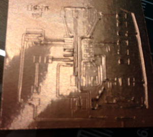
Rob (our fantastic TA) came by to help adjust settings as well. He said the traces were way too thin to easily weed so we tried tricking the fab modules into thinking the tool diameter was smaller to get things spaced more reasonably. We also tried scaling up the png in the fab modules just a smidge to see if that would make things easier. To no avail, still had the problems of traces being dragged up. The sad and anticlimactic conclusion is that I need to redesign my circuit and beef up my traces paying close attention to the design rules in the tutorial. Weird angles are actually harder to weed, and space components a bit farther apart so you can get into places with your tweezers more easily. I definitely want to revisit this in the near future because I believe my stained glass circuit will be beautiful. Spent hours on this, But for now I am sticking with the milling machine until I can redesign my circuit.
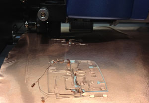
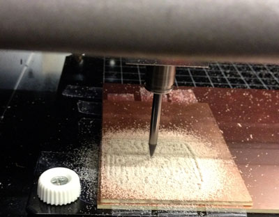
I changed the sacrificial layer of copper, cleaned everything off, loaded the png in fab modules, inverted the png, changed the cut depth to -.2. Zeroed x, y on milling machine. Placed 1/64th endmill in, Lowered z height on endmill so there was a finger tips width in between the top and bottom so there'd be room for the endmill to move down. Zero the z height and start milling. I zeroed the board a bit too close to the edge so when I went to cut out the board I was worried that the cut out would go off the board so I left the board bigger and didn't cut it out. This definitely should be redone.
A few of the traces came out as touching so I cut away the copper to keep separation in between traces. This should be changed in my design.,/p>
Put links here Coming Soon
Coming soon!!
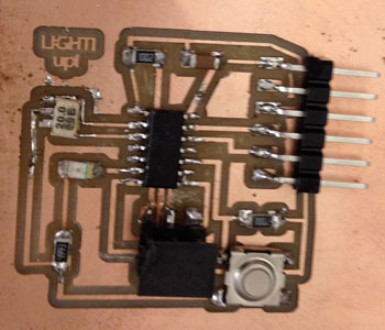
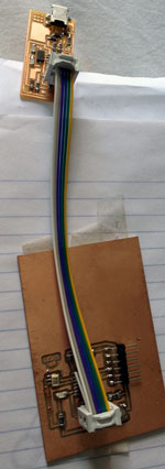
Coming Soon! Finished, stuffed Board, needs to be programmed to do stuff!!!!
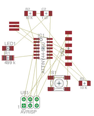
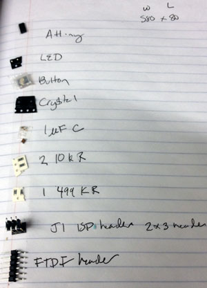
For designing: Eagle Photoshop Inkscape Corel Draw Gimp For Making: Vinyl cutter Modela milling machine Materials: copper sheet, glass, tweezers, components to solder, FabISP from week 2,
I am not yet indoctrinated into the coolness that is embedded programming. This will happen soon.
Copyright 2013 Kathy Sinclair