This week's assignment is to make a press fit construction kit from cardboard - an exercise in going from 2D to 3D by creating a set of parts that can produce a wide variety of 3D shapes. I've done some similar projects with a 3D printer and straws (here, here, and here), so for this week's assignment I wanted to go a little bit further and try to bring in the concepts of spatial computing into my designs. That is, instead of using identical parts to construct a regular, symmetric lattice, designing a set of parts with information embedded in their geometry. This way, the lattice assembles in meaningful, programmable ways.
The inspiration for this project comes from the paper "Algorithmic Self-Assembly of DNA Sierpinski Triangles" by Rothemund, Papadakis, and Winfree (image above). In the paper, Rothemund et al describe how they created a set of DNA tiles - modular pieces of DNA with four exposed "sticky ends" - that spontaneously assemble into Sierpinski Triangles. A set of four tiles was designed to exhibit the behavior of an xor gate for four possible input states. When placed in aqueous medium and allowed to self assemble, sierpinski triangles are the logical spatial output. Here is a great video that explains this in more depth:
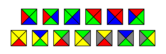
This concept is generalized in Wang Tiles, a set of tiles that must be arranged in an order dictated by their sides (image below). Tiles may not rotate, and tiles may only touch other tiles if their sides the same color. You might recognize these from your childhood - I think I might have played with a toy inspired by Wang Tiles as a kid.
Though these logical tiles have some computational merit, I'm more interested in their potential for fabrication: controlling the patterning of features across a material. If certain tile types can be engineered with special properties (conductor/insulator, photocurable/soluble, etc), then it might be possible to self assemble useful structures on very small scales.
Some work in assembling DNA in 3D using modular bits is being done. DNA bricks is an idea to build 3D structures of DNA from small pieces that can only fit together in pre-defined ways:
This process has generated some nice results, but I'm not convinced it will scale well for larger geometries. Since each voxel requires a unique brick type, the amount of bricks needed to make an N x N x N cube is N^3. Requiring so many different raw materials for one synthesis increases production costs and may reduce the specificity of brick binding, especially as we try to build larger structures. If we could somehow design geometries in a way that can be assembled by a smaller set of bricks in a programmatic fashion, the idea would be much more expandable.
In this week's project, I wanted to explore the concept of self-assembling logical bits in 3d, using cardboard as a model. I started by thinking about building cube-like structures (3 inputs + 3 outputs = 6 faces total) that fit together as voxels in space, but had a hard time designing something elegant from 2d sheet that met all my requirements without too much complexity.
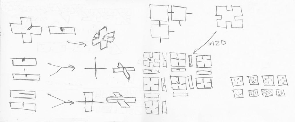
After some searching, I landed on the GIK design as a way to bring 2D into a 3D lattice with sufficient interconnectedness. As I started looking at GIK, I realized that I'd already used it once in another project - a set of modular shelves I built last year based off this design (GIK using right triangles instead of squares). One convenient property of GIK is that each module is a flat square, with four points of connection; this meant I could stick to the 2 input / 2 output model from the DNA tiles/Wang tiles examples and limit my tile set to only four tiles (4 possible input states).
I began by building a scripted, parametric design tool for the tile design. Last week I used RaphaelJS to do some 2D graphics and animation. This week I'm using Raphael, Raphael.Export, and the Blob API to design and export SVG files to send into the laser cutter (download only working in Chrome so far). I'm also using ThreeJS to render the assembly in 3D on the canvas to simulate what the "programmed" structure will look like (not quite done yet, but reeeeally close). ThreeJS is a little more complicated than Raphael, and I've only used it once before, so this was a learning experience (here are the docs). Note - I won't be using it this week, but three.js pairs nicely with THREE2STL to export stl files directly from the browser. I used TrackballControls.js to add interactivity (pan, zoom, rotate) to the 3D model. I'm also using JQuery and JQueryUI for some UI components and helper functions.
The design tool is below (code here). The 2D tile editor lets you program your set of tiles. One set of tile consists of four main tile types (for the four logical states of the inputs), four edge pieces, and one corner piece. The input bits on each of the tiles is highlighted in yellow - these do not change. You can toggle the output states by clicking on it in the editor. Notice how the svg output updates when you toggle the output state of a tile. In my system, the state of a tile input or output is controlled by the depth of the notch. When constructing the lattice, short notches may only fit with deep notches and vice versa for the alignment to work out. This constrains the way that tiles may attach to each other.
The parameters of the svg output are controlled by sliders and inputs. The download button will save a copy of the svg output to your computer (again, Chrome only, I'm not sure what's up with that).
The 3D canvas is just a few lines short of showing a simulation of the assembled lattice (so close!) For now it shows the assembly in a bunch of random colors. When it's done, it will not show every tile in the lattice, only the tiles highlighted in red in the 2d tile designer. This will draw attention to significant substructures of tiles within the lattice. You will be able to click on a tile in the 2D editor to toggle its visibility in the 3D simulation. By default I've highlighted all tiles with LSB = 1 in red. The 3D canvas is interactive, drag to orbit, scroll to zoom and right click (two finger click on trackpad) to pan.
Notch Width:
Tile Width:
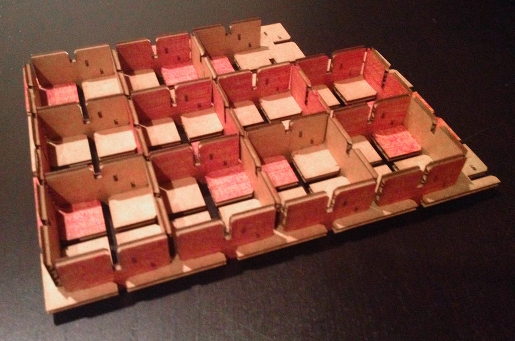
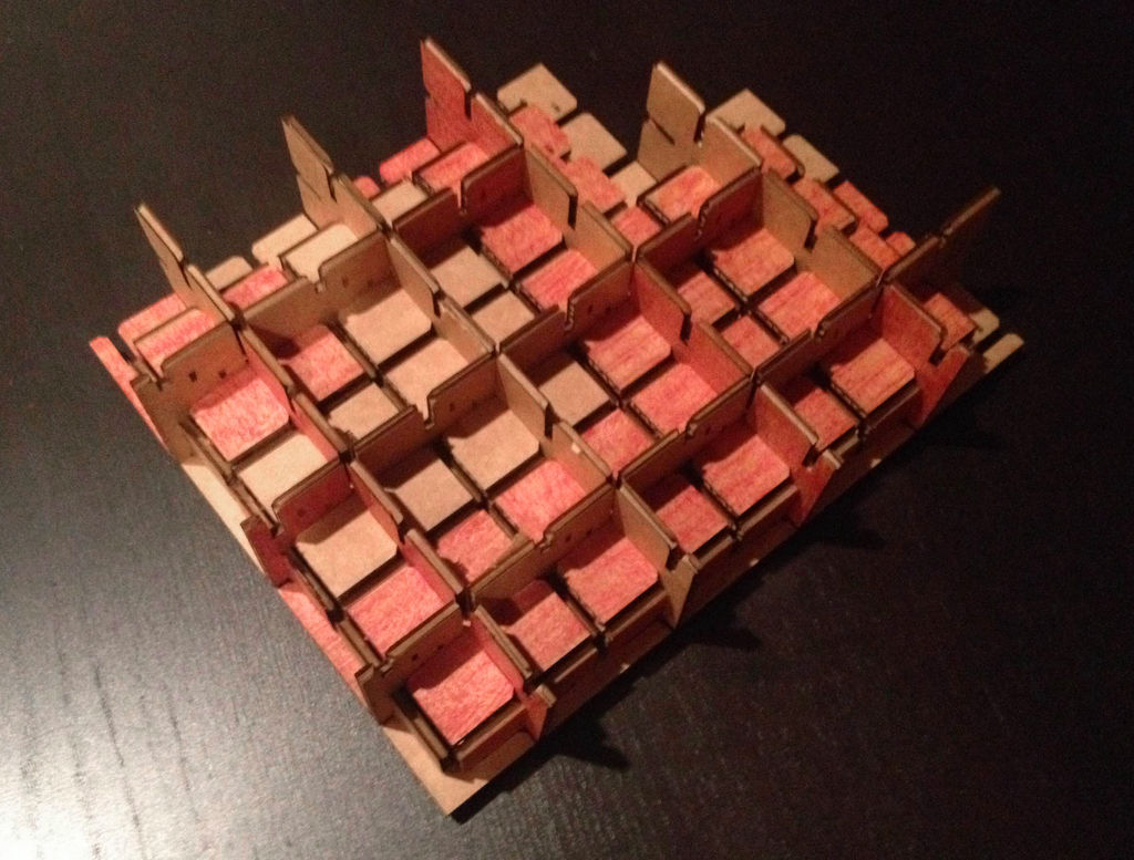
The tiles I cut are shown by default when the tile design tool loads. Each tile is acting as a summer, outputting the sum of the two input states to the MSB and LSB outputs. My tiles of interest (shown in red) have an LSB = 1. I imagine that these tiles will highlight a structure on my lattice that shows bit addition happening across space - though it's not entirely intuitive without a simulation or a physical model what that will look like. I designed my edge and corner tiles as though their missing inputs were 1's.
I laser cut my files on an Epilog laser with a 0.155 notch width. I cut the MSB and LSB tags with 5% power and 100 speed so that they were only etched on the surface of the tiles.
As with Wang Tiles, the orientation of the tiles during assembly is very important. I assembled all my tiles starting from the bottom corner tile, building out and up so that MSB was always on the top edge (vertical tiles) or pointing in the direction of +y with the letters visible from the top (horizontal tiles). Though it seems like this orientation constraint would break down in a self assembled lattice, it is really just a limitation of the cardboard model. I could have created 4 states in the notch depths (2 for inputs and 2 for outputs) that physically prevents input/input and output/output pairing, but the cardboard pieces were just too small. The differences in notch depth would have been subtle, I think it would have been confusing for the human assembler.
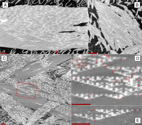
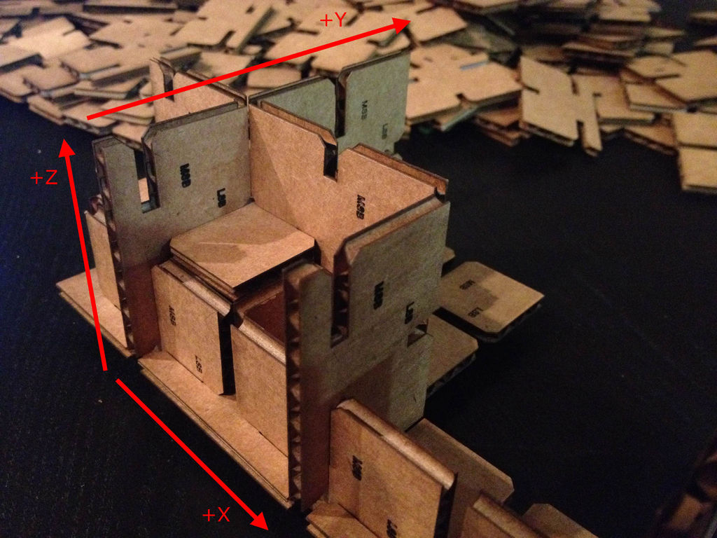
I colored certain tile types red (tiles with LSB = 1) and assembled them until I ran out of tiles. Unfortunately, I ran out much sooner than I'd hoped. Though I started to see some emergent patterns in my lattice, I didn't have enough to identify exactly what was going on - and what it had to do with summing bits. Another problem is that the opaque cardboard material obscures the inner structures of the lattice, so it's really not the best material for this type of model. This would probably look great in clear and colored acrylic. Here are the patterns I saw on the first two layers of lattice:
I'd like to continue thinking about this project and maybe work it into some future week's assignments, I think there is still a lot to explore. Some things I'm interested in:
more tiles - I didn't cut nearly enough tiles to fully explore the model I've got. Since I didn't know which tiles would get used up the fastest, I cut equal amounts of everything. Turns out I ran out of a few tiles very quickly and had a lot of extras of others. I'd love to cut out a few more tiles when the laser isn't so busy.
exploring more tile combinations - I've just recently got the simulator up and running, it's a great tool to design in before committing to a physical model. I want to spend some time with the simulator looking at the possibilities, seeing if I can find some interesting emergent structures.
different lattice structures - this week I've modeled this process on GIK, but what would this look like on other types of lattices? Systems with voxels that have three inputs and three outputs? other geometries (not based off a cube)?
modified visualization - it might be easier to understand what's happening in the GIK lattice if I model each tile as a node instead of as a flat sheet in my 3d visualization.
>2 states - so far I've been working with a binary state system. How would the output differ if there were more than 2 possible states for each connection?
non-deterministic (probabilistic) algorithmic self assembly - In all my examples so far there is exactly one tile that can fit into any given space, but what if you designed some redundancy in your tile set? If you created two tile types that had the same input states and mixed together both sets of tiles into your mixture in equal proportions, in other proportions?