Electronics design
This week the assignment was to take a simple board with a programmable microcontroller and add a classic button switch and an LED to two different pins. I used Eagle to design from scratch the original board and then add the extra components.
In Eagle, I created a new project and a new schematics and board files. I had them opened from the beginning and initially i worked on the schematics level only (importing parts, labelling pins, creating connections). This way all the information was transferred to the board file. I hooked up a red LED and a 500 ohm resistor in series to pin PA7 (500 ohm at 5V delivered from the IC will produce a current at ~2mA level which fits the LED specs) and I placed the button between the ground and pin PA2. I will have to activate the pull up resistor in the IC. In that case when the button is open, there will be no current through the resistor and the pin will be at a higher voltage. When the button will be closed, the current flowing through the pull up resistor will drop the voltage at the pin.
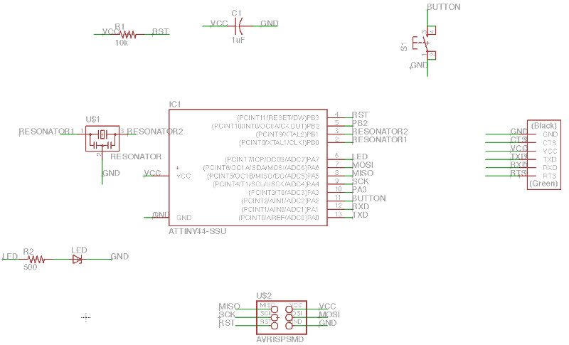
Once that was done I moved on to the board and arranged the parts in places and then routed the connections. In retrospect using autorouting would have been much faster but with a board this size it wasn't to problematic. The DRC ability to verify the design rules was useful - it revealed that i could not fit 3 16mil wires between the IC pins so i reduced the size of the wires to 12 mils which in retrospect was cutting it close.

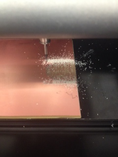
To get the outline I copied the png image and drew a suitable outline around the board and then removed the wiring:

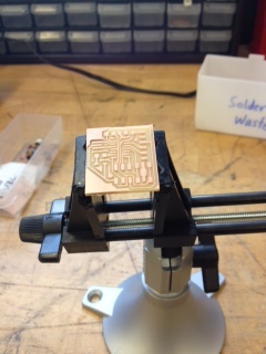
When it came to cutting i realized that i could not adjust the origin freely - effectively the origin of the cut is at the lower left corner of the png file. I was lucky as there was enough copper pcb board that my cutout was just able to fit:
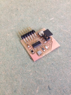
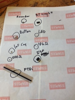
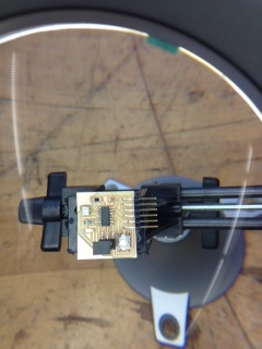
I was then ready to stuff it:
Which went much quicker this time:
And here's the final product: