electronic design
the project
This week’s assignent was about designing an electronic circuit (hello.ftdi.44.echo) using a CAD-program, milling the board and stuffing it. As a minimum additional requirement an LED and a switch should be added. Like many of my peers I decided for the EAGLE PCB CAD software for some reasons; it is freeware, as long as used for non-comercial puprose only, a maximum board size of 100 x 80mm, and two layers – limitations which are more than acceptable for our purpose. Installing Eagle is memory efficient and steightforward even in Windows.
electronic design in eagle
Since I was a freshmen in designing Eagle, I took the three basic tutorials on the sparkfun-learn page
1: Setup and Install Eagle
2: Using Eagle Schematic
3: Using Eagle Board Design
I found them essential and helpful, and with some hours of trial and error they enable your first simple board design. In addition to the fab library (change extension from “txt” to “lbr” and “commit” by right mouse click and “use all”) I also imported the SparkFun library (ZIP-file in the Eagle library directory); it has many useful parts I used the USB-connector (USB-A-PCB), the GND-symbol, the Button, the Vcc, as well as the Frame. Figure 1 shows the Schematic-Window of my circuit design (hello.ISP.44 + LED + Switch).
The basis for this assignment was the hello.ftdi.44 layout ( FTDI stands for Future Technology Device International), as shown below.

circuit Design in the schematic Window
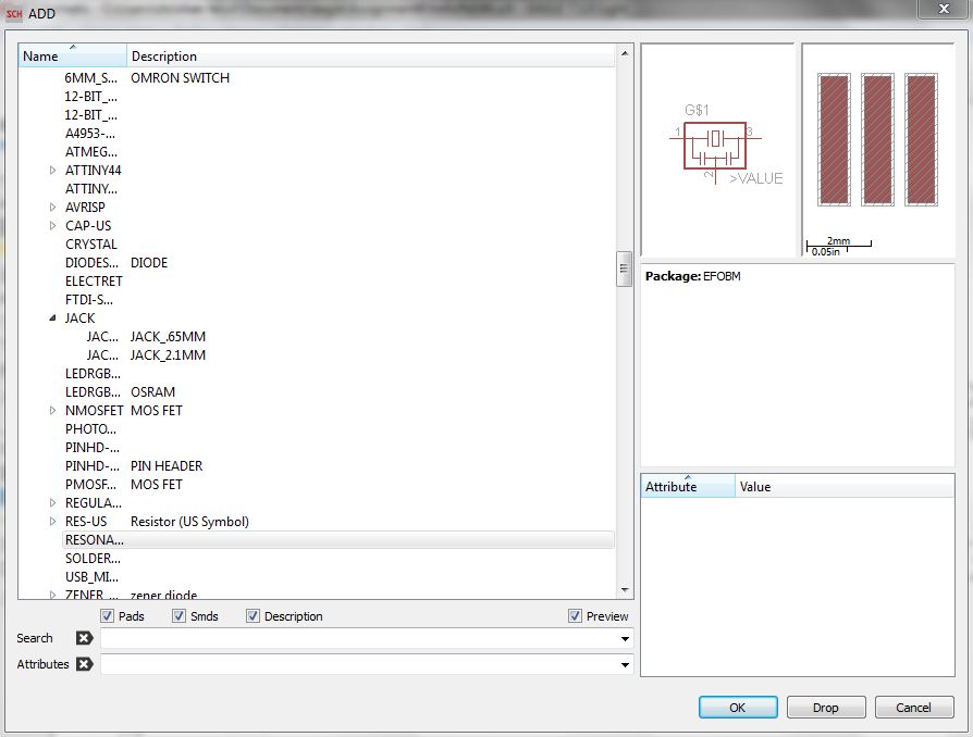

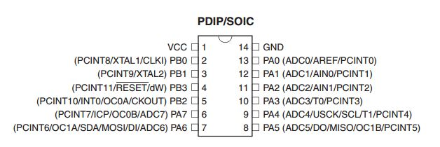
figure 1 shows how to add an electronic part from the fab.lbr in eagle: In this case the 20MHz clock resonator; figure 2 shows the schematic representation of the hello.ftdp.44 circuit: the input from the ISP (J1) on the left, the added LED-Pull-up resistor-switch combination for checking Vcc; the 20MHZ resonantor, the 14-pin IC1t44 microprocessor in the center, and the FTDI-output (J2) on the right.
checking the circuit
Checking the circuit with the “show” tool in the Schematic Window is highly recommended, I may case many connections which appeared correct identified as not connected in this test. The suggested troubleshooting “deleting and re-connecting” sorely doesn’t work all the times; I identifies deleting parts and reloading them from the library often helps - it seems somehow to be related to the raster-positioning. As noted in the tutorial, making connections only do the very beginning (avoid overlaps) of a pin is definitely important - you will recognize if the connection was made correctly if the line isn’t continued after clicking the left mouse button. Finally, when you have checked all connections with the show tool, a successful test should look like shown in figure 2 (test of ground-connections, note also the connected labels). For the current limiting transistor for the 1206 LED (red, 1.8V, 10mA) I choose 500 Ohm (> (5-1.8V)/10mA=320 Ohm).
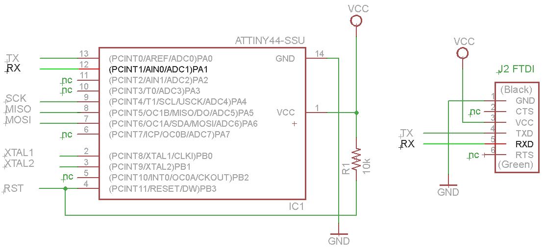
figure 3 shows the checking of the circuit design in the schamatic window by the show-buttom: all RX-related connections are highlightes in red and light-green.
board design in the board window
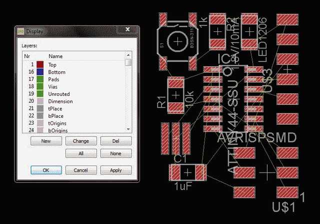
After the circuit design was approved, I started the board design in the so called Board Window; Since I wanted to solve the puzzle by myself, I didn’t take advantage of the auto-router, which is typically used to assist with more complex designs. Avoiding too much "airwires" right from the beginning helps, als turning parts can sometimes solve the puzzle. Starting to wire the more komplex parts and leaving GROUND and VCC to the end seems alsa practical, since the multiple connections could be solved with a kind of frame at the end. As with the “show” functions before, Eagle provides two very helpful tools checking the board design before manufacturing; 1)missing connections could be identified by the “Ratsnest” function – even a small missing connection can easily be identified by disabling all layers except lacer 19 (“unrouted”). After that I performed the Design Rule Check – I uploaded the SparkFun design rules - two hard to spot errors could be identified and cleared. The final board design is shown in figure 3.
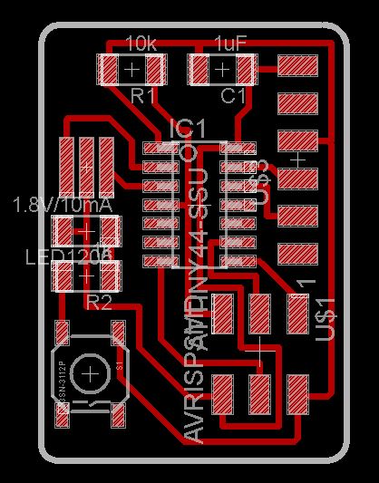
Ratsnest: "Nothing To Do!"; Design Rules Check: "DRC: No Errors" - The Board is fine (left); right: Adding copper to the board for the GND-surface (Draw a "Polygon" over the Dimension Box, stay in Layer 1, select a insolation distance, e.g.0.012", "Name" (label) it - it this to GND; "Ratsnest" shows the new surface).
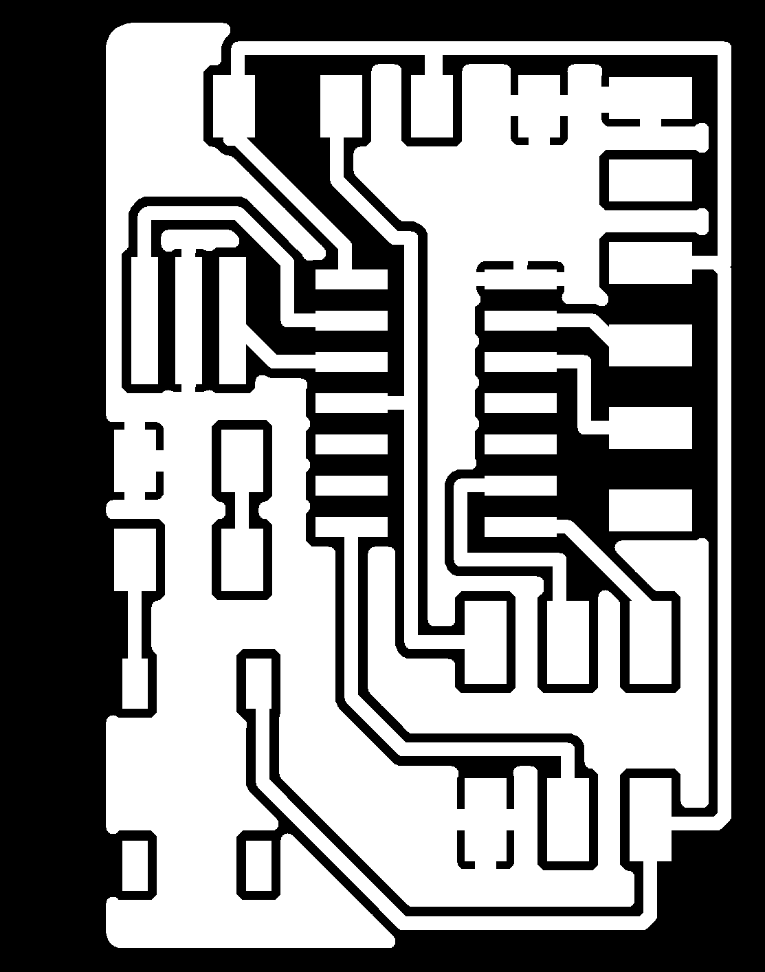

figure 5: Ready for fabrication with the Modela; the PNG-files of the circuit (layer 1, left) and the dimension (layer 20, right); you receive them by exporting them as an image (select 1200dpi, monochrome).
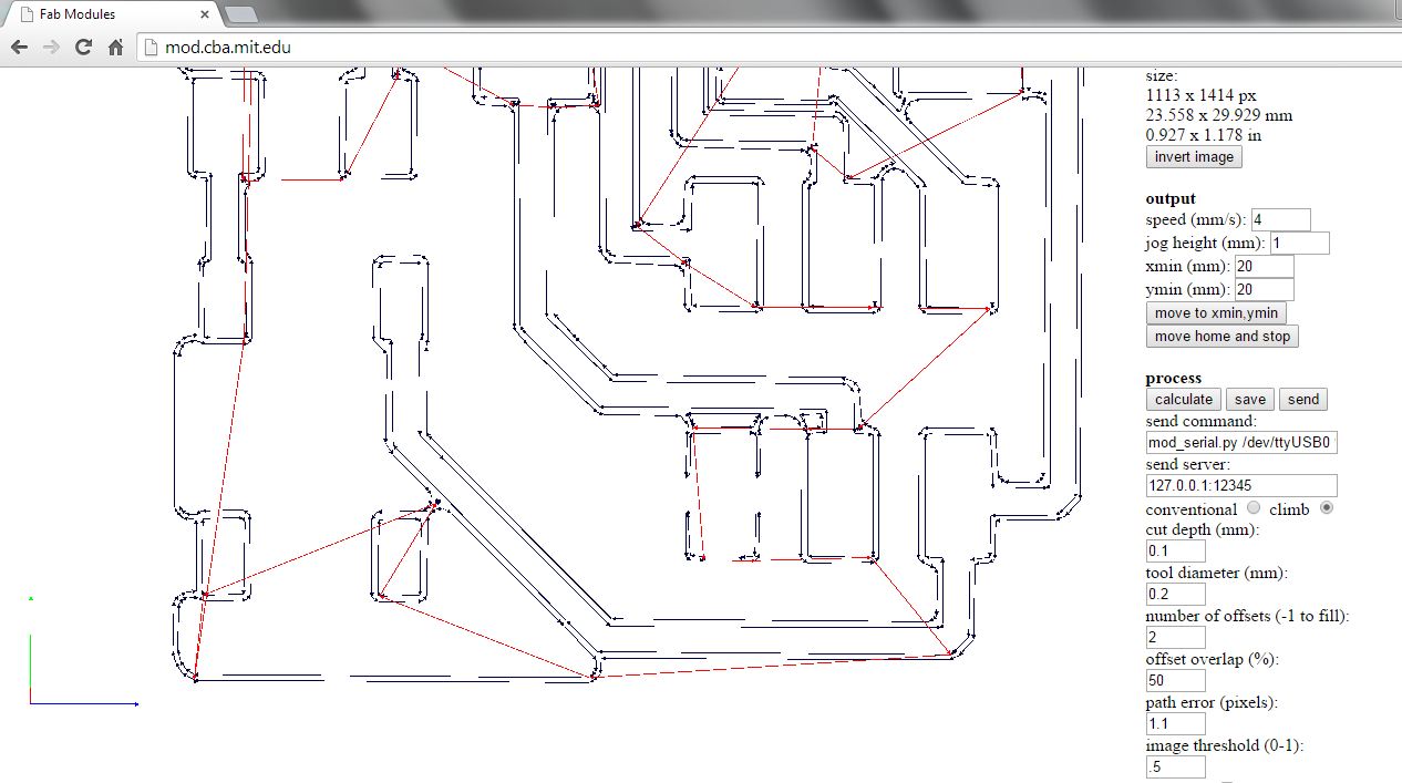
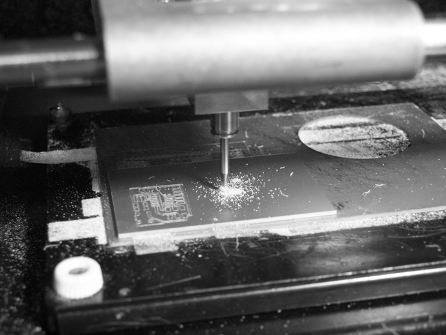
figure 6: top: checking the milling route using the fab lab module; the calculated path for the 1/64" mill (=0.4mm) would lead to short-cuts, so I set the tool diameter to 0.2mm, as wellas the number of offsets to 2; bottom: the modela in action (using a 1/64" mill for the circuit, and a 1/32" for the border).
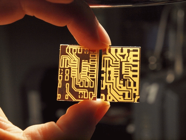
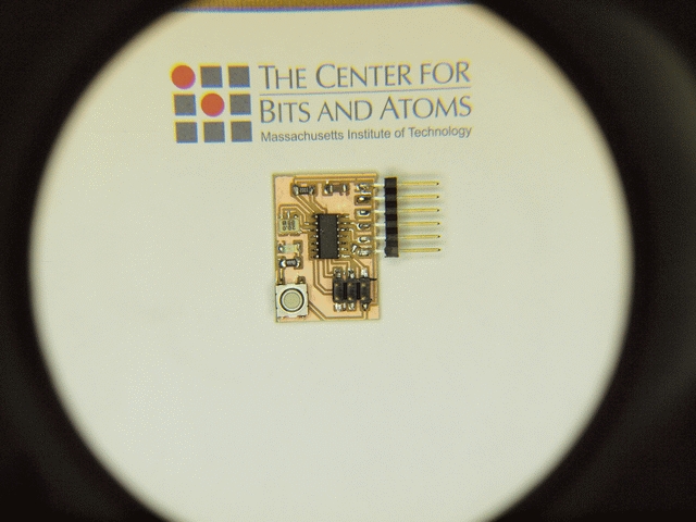
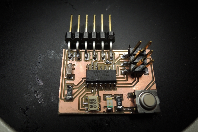
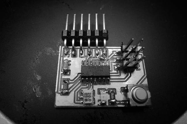
figure 7: left; the two bords after milling; with the one left I used the polygon-function from Eagle and labeled it to ground - it safes milling time, however, I had to set the tool-diameter to 0.2mm to avoid shorts; on the other hand it can also be harder to stuff the board. With the right (conventional) board you can see a short under the mikro-controller; right: the stuffed board hello.ftdi.44 including a switch, LED and currentlimitting Resistor.