The first step of the adventure is to mill out the board on the Modela. The board is stuck down with double-sided tape.
You can fit two boards side-by-side on the "small" pieces of PCB stock, if you very carefully align the bottom left-hand corner of the stock just a little left and down of the machining origin, (20mm, 20mm) by default.
It's important to keep the board as level as possible. If the substrate is too damaged to get a good level over the whole mill area, the substrate should be replaced. Otherwise, you may find that the bit gets through the copper on one side easily, but only scratches it on the other!
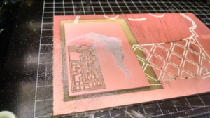
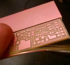
Fresh out of the Modela, the dust pushed aside to reveal the crisply rendered board.
Be sure to vacuum up the dust carefully, to avoid gumming up the internals of the Modela.
Unfortunately, I found that the mill depth was not quite large enough, probably due to an inaccuracy in my Z-axis zeroing. A wafer-thin layer of PCB was left over after the machining process finished. It was difficult to tell that this was the case before it was removed from the machine.
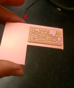
Even after routing the edge, the board is not free from the PCB stock, but remains connected by some webbing
All is not lost, however; even though I had already removed the board from the stage, so that there was no possibility of re-machining the path, this is a recoverable mistake. I'm sure you can imagine what needs to be done.
One subtlety, as we free the board: don't cut, but break. Cutting, e.g. with diagonal cutters, will create high stresses within the material which could cause a crack to propagate through the board, even though the thin webbing around the edges clearly offers less resistance. Use pliers to stress the board until it breaks; then you can be sure the cracks will follow the path of least resistance.
Align the long edge of the pliers with the edge, to avoid stress concentrations.
Maybe this is overkill, since this is not a terribly brittle material, but it never hurts to think about stuff like this.
Mistake easily recovered.
See? There's definitely room for someone else's board to be cut out next to this one.
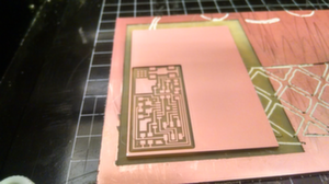
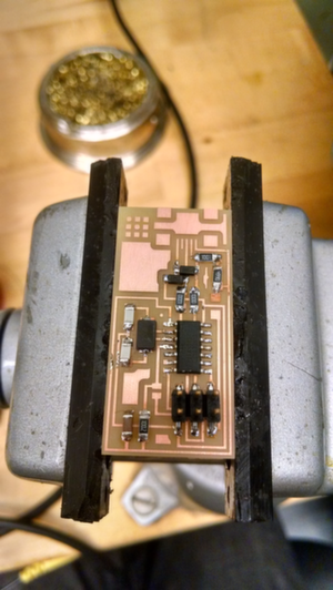
Now that we have a pretty milled PCB with pretty milled traces, we can start soldering. I recommend setting yourself up with a nice board clamp in front of a computer, so that you can continuously check your work against the schematic and the board image. Both of these resources can be accessed through the class page, under Electronics Production (the "board" and "components" links).
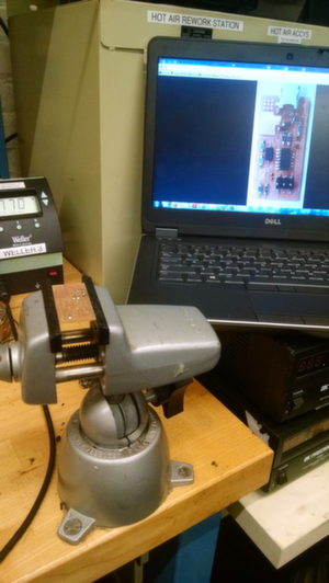
Computer within easy view, board clamp saving you hands.
The smallest, fiddliest components should be soldered first: the resistors, capacitors, and diodes. If you do the big stuff first, it will be in the way when you do the fiddly stuff. Makes sense, eh?
A quick note on resistor labelling: if there's an R in it, read it straight off as if the R were a decimal point; otherwise, the last digit represents the power of 10 by which the other digits should be multiplied. For example:
45R5 = 45.5 ohms
1001 = 1000 (1K) ohms
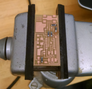
Resistors, capacitors and diodes go first. Here, all of the resistors have been soldered in place.
Go ahead and finish up with the caps and diodes. Remember, the diodes have polarity (in fact, a wise one might say that's all they have!). The faint line running across the body of the diode indicates the cathode, marked with a 'C' on the aforementioned board schematic.
Next comes the ATTINY microcontroller. Remember, the little dot over a corner pin indicates pin 0; in this design, it goes in the top left. Tack this pin down with a quick little blob of solder, then do the same for the diagonally opposite pin; these steps mechanically align the board. Then begin soldering the pins in earnest.
Don't be afraid to pour solder all over these pins. Even if you significantly bridge them, you can go in with the copper braid afterward, and all you'll be left with is beautiful, minimal joints. This can be a very effective time-saving strategy. Just don't solder the braid to the board.
Here, the ATTINY IC has been soldered in place. I also did the 6-pin header right before I shot the picture (after the microcontroller!); it should give you no trouble.
It's good practice to go back and re-melt the two pins you used to tack the IC down (top left and bottom right) in order to relieve any stresses that may have arisen during soldering.
Great, time to do the USB port. Again, think critically about alignment. The first step is to tack one of the pins down, just as we did for the IC. This will align the actually important electrical connections with the traces. However, now your board is vulnerable. After all, if you happened to bump the port with the iron while you're working, that one tiny trace is probably not going to bear the torque well, and you may be looking at an extensive cleanup effort, if not a full redo. Before you manipulate it further in the process of soldering the other pins, take a moment to mechanically anchor your port by soldering the four large outer pads.
Now that you're protected from costly mistakes, go ahead and solder the other pins. Again, pour that solder on thick, and clean it up pretty with the copper braid.
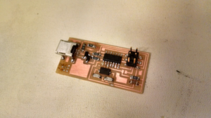
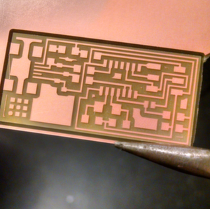
That's it! The board is done.
Hope you've gained something from this walk-through, and good luck completing the project.