I relied quite heavily on the pages of past students and online tutorials this week.
I was unable to make it to the Eagle tutorial this week, and so, computer aided circuit design required a bit of self teaching. I found the first half of this instructables to be quite helpful.
To begin, I downloaded Eagle which was free online. Then, I created a new project and a new schematic. I added the fab library by clicking "Library" > "Use" and selecting it.
Now, it was time to add the components. I added the ATTINY44, the resonator, the button, the LED, the ISP header, the FTDI header, one capacitor, two resistors,
seven ground symbols, and six VCC symbols. All of these were found in the Fab library except for the LED, the capacitor, the resistors, and the ground and VCC symbols.
The search function is a little weird to use when adding components. For example, the ATTINY can be found by search *TINY*. I found it helpful to do an empty search
and just look through the entire fab library a few times. Once everything is placed, it's time to connect everything. Using the net tool, you can click one port,
drag to another port, and create a connection. This tool only makes right angles, which is very nice for clarity. However, once you use the move tool, all angles are fair game.
I began by connecting each thing manually. I used the move tool early on and the schematic got kind of crazy as seen below...
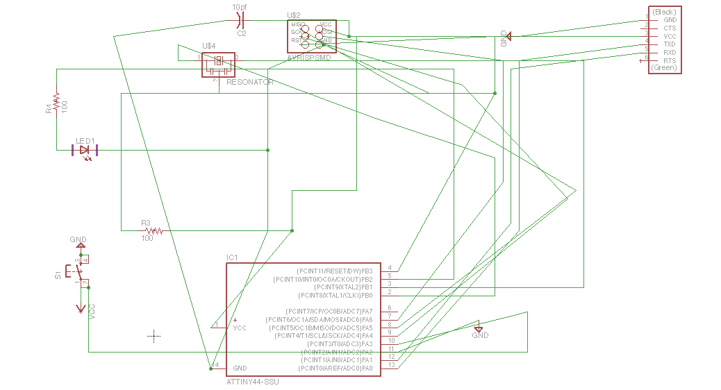
It is okay that the lines cross, as long as there is no green dot to indicate connected wires. I decided to go to the next step with this schematic.
By clicking "File" > "Switch to Board" you can begin to set up your board for milling. After some playing around, I realized that my schematic was probably wrong.
It was too messy and confusing to fix, so I decided to just start over again, this time naming connections and keeping it neater. This method can be done by creating a small net
off of each port. Then, right click one, name it, and label it. Ports that are given the same names are connected together. Once it was redone in this way, it looked like this:
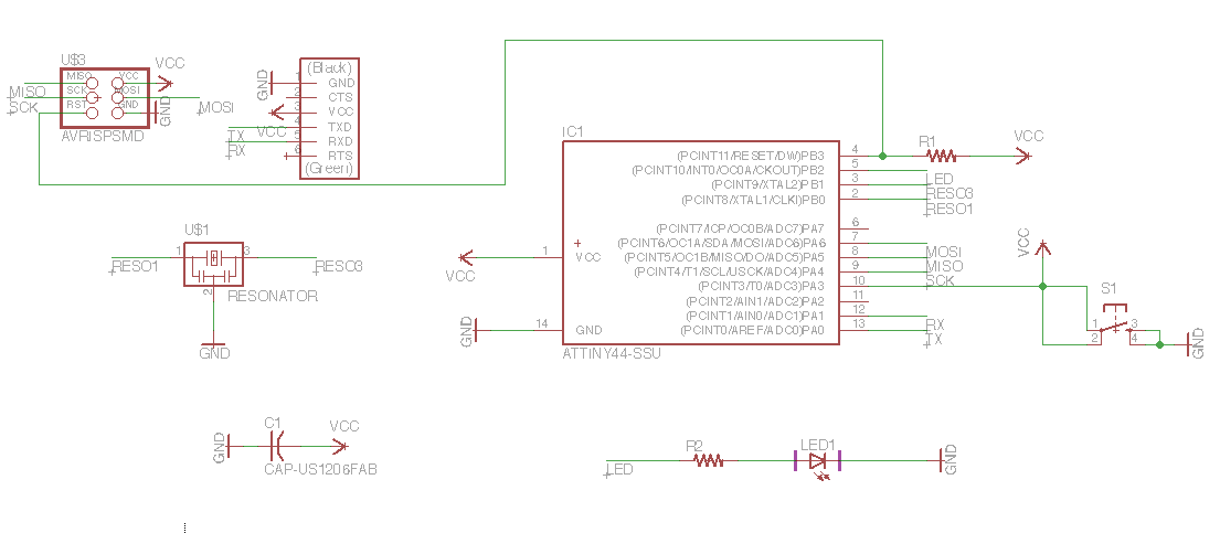
Much clearer, and more editable. I switched back to board mode. Yellow lines appeared, connecting each component as instructed by the names. Following the
instructables guide, I moved each component into the white outline with the move tool. I just tried to make as few lines cross as possible in placing the components.
Then, I used the "Ratsnest" tool. This redraws the yellow lines based on the placement. I then ran the "Autoroute" tool. After autorouting, I clicked evaluate.
This highlights any connection that could not be routed. I had one line that could not be routed, so I moved some things around and auto-routed again.
Then I had several things that could not be connected. After several iterations of moving and autorouting, I had a 100% connected circuit. I thought the wires looked
too close together, so I used the move tool to move some of the auto-routed lines. Then, I loaded the design rules by clicking "DRC" and then "load." I ran a
design rules check and it pointed out that my outline was too close and that some wires were way too close. I moved some things and re-ran the design check until it was okay.
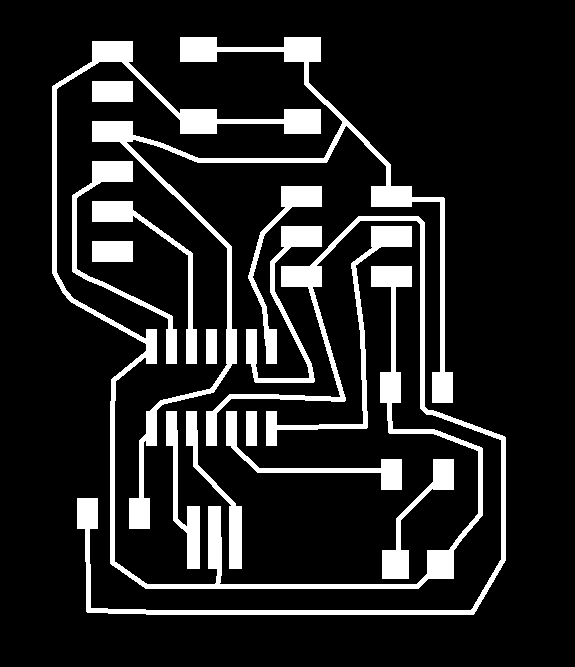
Now, I needed to prepare the image for the Modela. I ran the commands "display none" and then "display top" so that only the pads and wires would be shown.
I clicked "File" > "Export" > "Image" and then saved it as a .png with 500 dpi. This saves it as a red trace on a black background. Then, I uploaded it in a paint application,
turned all of the red to white and saved it again. Here is what the file looks like:
Finally, I created an outline file by simply drawing a white rectangle around the entire board, deleting everything else, and saving it as a separate file.

Now, it's ready for the fab module to be milled :)
I uploaded both .png files on the fab module and set the 1/64 end mill to go. I just had to change the dpi setting to 400 to match how I exported the image.
It cut nicely on the first try. I just noticed that some of the tight corners were left touching other connections. I just had to scratch away a few remaing slivers of
copper afterwards to fix this. When I cut the board out, I did not invert the outline image, so it treated the outline as a wire. Fortunately, I had left enough
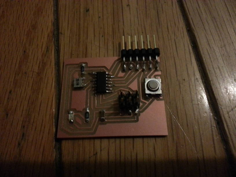
clearance outside of my circuit for it to not ruin the circuit. It was very close though. Finally, I just soldered the components on.
Below is a picture of the completed board: