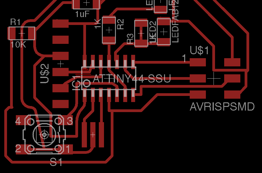
I spent the large bulk of this week's assignment learning about Eagle, and in particular learning how to generate schematics and boards. I relied on Ermal's schematic from last year to help guide me through the process. I added all of the Fab components and made the schematic without much trouble (adding a second LED in the process).
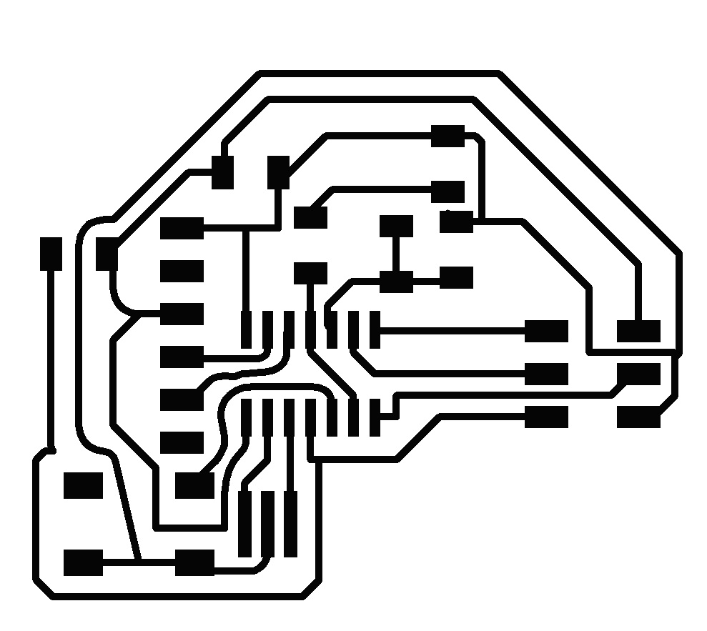
The routing, however, did not go as smoothly. It seemed for many, many hours like there was no solution to this puzzle. Here are some fundamental mistakes that I made and some tips to completely avoid them!
Mistake: Do not rely on Eagle's autoroute feature: my initial strategy was to lay out my pieces in a way that minimized line crossing, and then attempt to run Eagle's autoroute feature (with our milling machine's clearances of 17mil recorded in Eagle's DRC). I almost never found a 100% autoroute solution, which continued to lead me to believe that I needed to find another orientation for my parts.
Advice: If you do run Eagle's autoroute feature and don't get 100%, you can sometimes still manually resolve the last few issues by either adding in 0-ohm resistors or by manually finding a path. It seems like general consensus that by learning to become a good router you can outdo Eagle's feature. This strikes me as peculiar, and I wonder whether it's possible to further optimize the software for small circuits (such as by allowing it to add in 0-ohm resistors). Obviously, for complex and/or multilayered circuits, autorouting is still the way to go.
Mistake: Do not connect components in an arbitrary order! Eagle misleads you by showing you a line between the component you are trying to connect, and the shortest connection path. I arbitrarily started selecting components to connect and finding the shortest path.
Advice: SAVE POWER AND GROUND CONNECTIONS FOR LAST. I met with Jeff (TA) after many, many hours of failing to find a viable circuit diagram, and I think this was the key piece of advice that I had been missing. There are MANY places within your circuit where you will be able to connect power and ground. Save them for last!!!! Also, start by taking two key components and connecting them, then add the next, always saving power and ground for last. Wish I'd had this in mind from the start, as it could have saved many hours!Future HTMAA students who haven't routed before: take this advice in particular!
Bonus Advice: Do a design check before exporting your image. There were some regions underneath my processor that had traces very close together. Using the design check feature I was able to tweak those lines to minimize risk of impact when milling.
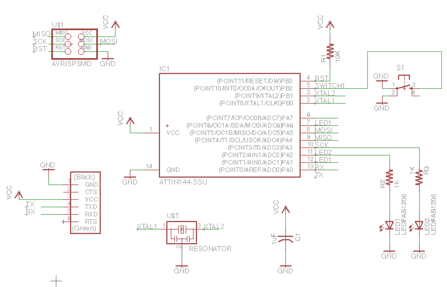
Above is the schematic that my circuit design was based off of. Finally with a workable design, I exported my image to PNG format (600 DPI) and went off to print the board.
More problems ensued. Firstly, my exported images suggested that my circuit would be something like 4x4 inches, which seemed much too big. I think it's because the exported images included a lot of buffer space. I had to crop my images to the same size and then set 600 DPI as the resolution in the fab module.
The first time I cut, the circuit was cut properly, but due to the cropping, the border cut a bit shifted, and did not cut all the way through (I think I accidentally set the bit size as 1/64 even though I did replace the tool, which may have had something to do with it.)
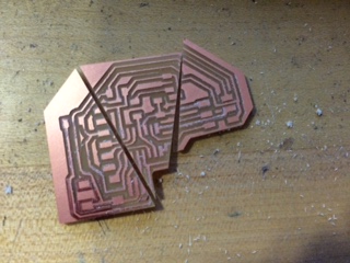
The next time, one quarter of the board did not cut deeply enough, so I had to recut with a depth of .15mm (instead of the default .1mm). This time, the border cut two giant lines through my circuit! I should have noticed this in the calculated path. Images are above. I don't know what caused the issue, but I resolved it by inverting the exported image in Eagle and regenerating the image. I then tried to recut the border of my first board by eyeballing the alignment, but didn't eyeball it well enough and part of my circuit cut off.
Getting Closer!
Third time's a charm (well, turned out not to be). I recut my circuit a third time, but the bottom left corner didn't get rid of all the copper. I increased my cut depth to 0.18mm and cut a third time. Still some copper left in the corder (I think the sacrificial layer was popping up a bit) but I might try to remedy with an exacto. While cutting the border, the board popped up and the drill cut into it a bit. I think some dust may have caught under the tape.
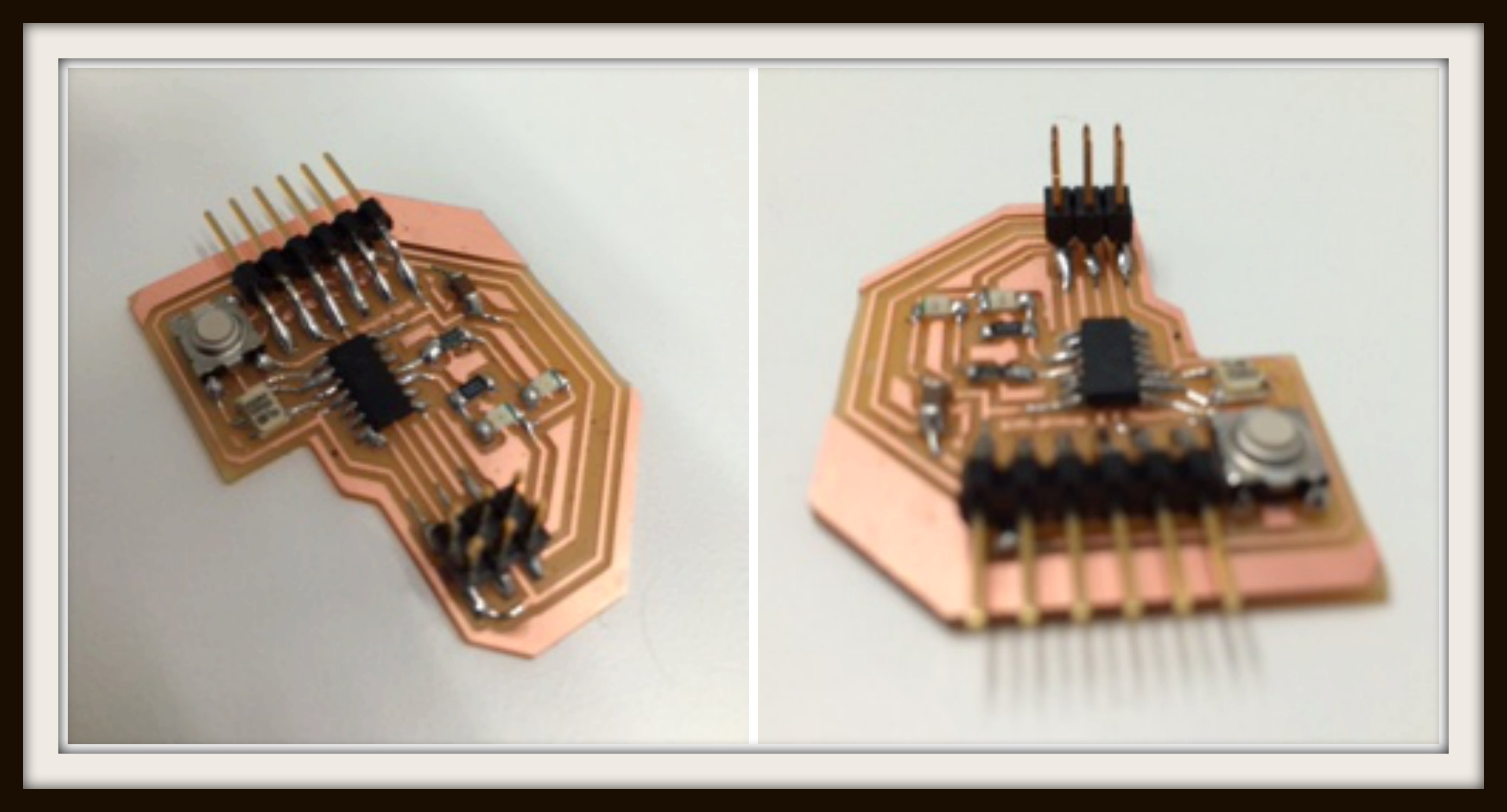
I cut a fourth time, this time in the back corner to avoid the area in the sacrificial layer that was popping up a bit. This time it finally cut smoothly! Soldering went completely smoothly since we'd practiced a lot a few weeks back.