 In the end, I ended up sorting out my confusing and
coming up with a schematic:
In the end, I ended up sorting out my confusing and
coming up with a schematic:
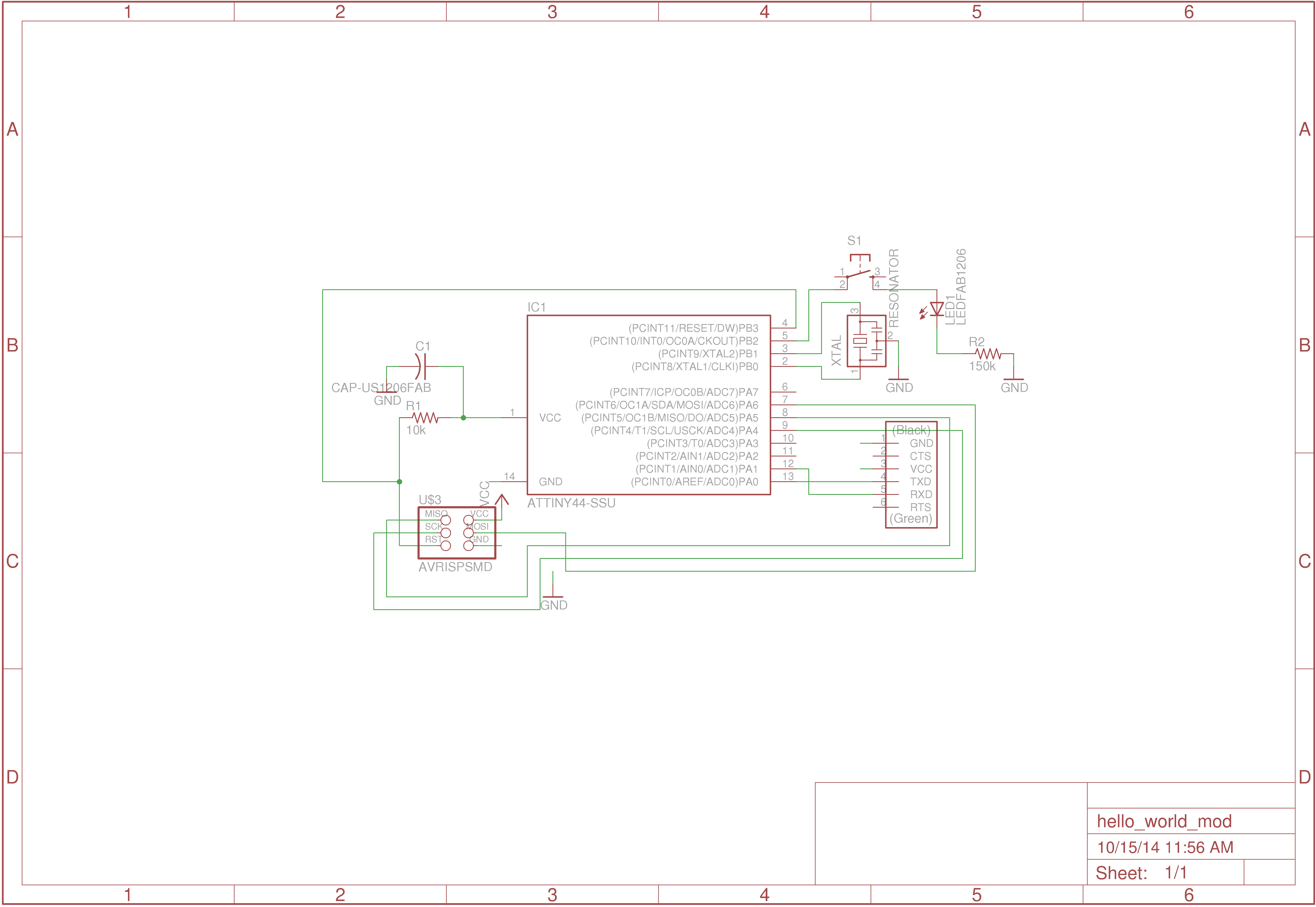
The extent of my experience with electronics is that I have programmed a bunch of microcontrollers, and that when I was very little I was given one of these circuit kits, which I proceeded to try and fail to build a computer out of. (Although I think I got binary addition to work, TTL remained a deep mystery to middle-school me.) Now, the tools are different: instead of awkwardly picking and placing pieces of plastic we do the same with symbols on a screen.
I decided to do this week's assignment with Eagle since I had heard of it before and it seemed like learning a standard hobbyist tool is a good idea. Installing Eagle was straightforward. However, using it was not. Moving objects requires a dedicated move tool. Moving a group of objects at once requires a "Group" action, a click on the "Move" tool, and then a right click to make sure the entire group is moved. I found it nearly impossible to select a component after a number of traces have been added to it, since the traces rather than the comonent would always be selected. You may notice some unnamed parts in the pictures; this is because I could not manage to select them in the UI to rename them, and I did not want to redo all of the connections.
Eagle is full of user interface decisions from a time when a mouse was an advanced new technology.
There were two troubles here. First, the original fab.lbr did not have single color LEDs. Instead, it only had an RGB LED with four connections, which I do not think my shop actually had. Luckily, someone made an updated fab.lbr with a single-color LED of the same form factor as a resistor. Thanks!
I also got fairly confused between crystals and resonators. The
hello world board has a component named "XTAL", which I assumed
meant crystal. However, the crystal component in Eagle did not
actually have three connections, as were necessary. I
was stumped by this for a while, and eventually remembered that
resonators serve the same purpose as crystals, and although
the symbol for resonator is large and confusing and looks
nothing like the symbol for crystal, the resonator's footprint
matches up with the traces on the hello world board.
In the end, I ended up sorting out my confusing and
coming up with a schematic:
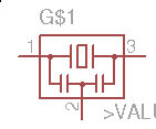
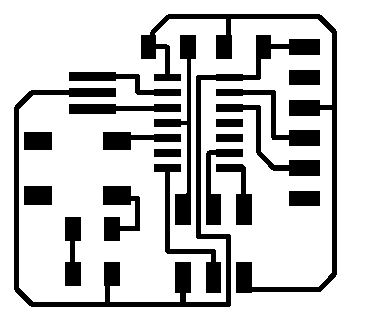
As you can see, I just added a button, an LED, and a 150k current-limiting resistor (value calculated using ledcalc.com), all in series.
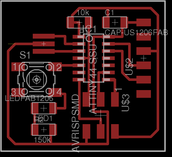
This part was frustrating. I switched into Eagle's board mode, and spent some time arranging the parts correctly. Then, I had many, many failed attempts at routing, all caused by slight misalginments of parts so that routes could not go through as in the hello world board without hitting various pads. The "readjust parts/reroute" process was repeated about six times before most parts finally had a route. However, then came the issue that the aspect of the hello world board where three wires go through lengthwise under the processor could not be completed in Eagle with the standard grid size. I ended up figuring out how to use the finer grid size feature. Note: you have to hold Alt to position your piece finely, then let go of Alt, then hold Shift and click to place your part. The latter part is necessary, as you can't place parts when just holding down Alt. Nonetheless, even this was not enough to pass the DRC rules regarding the 1/64'' drill bit; I ended up making these length-wise traces 0.014'' wide and setting the tolerance in the DRC to have a 0.016'' gap between pad and trace rather than a 0.017'' gap. Getting this process right took a while, but eventually it worked out.
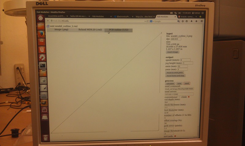
Finally, I followed the tutorial here
to make a PCB. I modified the commands to be more appropriate; namely,
I did "show none top" rather than "show none bottom ..." to view
the traces. The command line interface to eagle seems
quite straightforward.
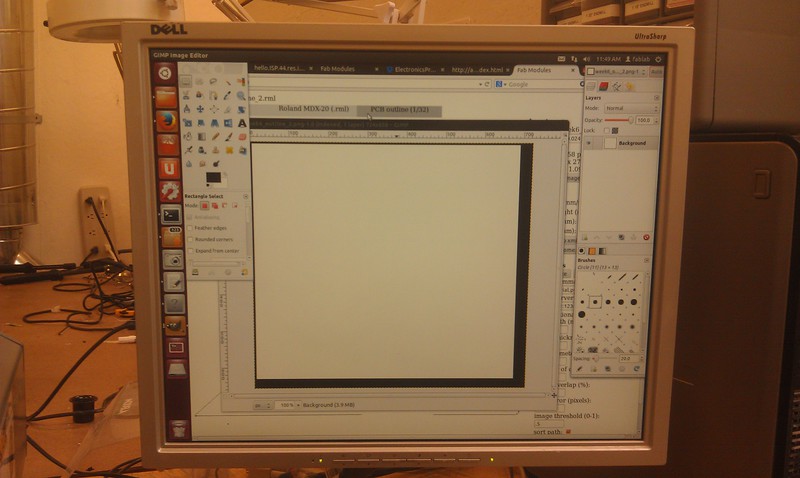
Milling the traces for the board was easy. However, I found that I had some errors with milling the outline. The error in the fab modules looked as below:
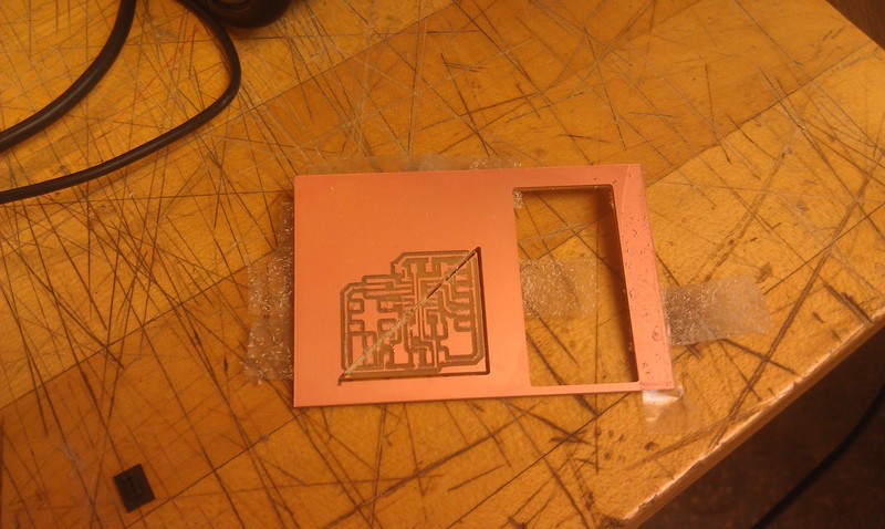
The board was cut diagonally in half before I could do anything! It was tragic and hilarious.
I remade the traces and opened up the outline file in GIMP. I realized that the way that eagle outputs PNGs (namely, it chooses the size it exports to be just big enough so that any layer would fit onto the image if that layer was displayed) causes the outline to have a white space around the edge of the PNG which differs in thickness depending on edge. Filling in the space with black solved the problem.
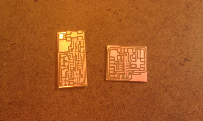
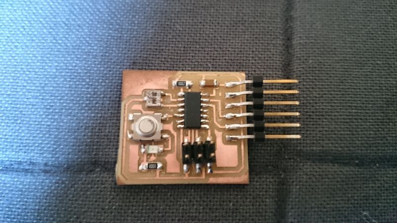
It was straightforward to stuff the board, although I had to take care to remember which way the button had to go: the only way to remember is to look at the EAGLE file. Finally, I have made my first self-designed PCB!