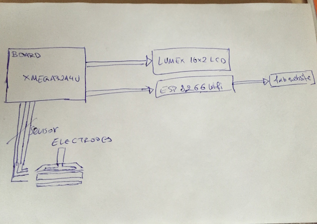
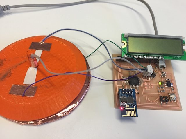
The project comprises of 3 main parts:
- The electronics board, housing an LCD screen, an ESP8266 Wifi module and an interface for the electrodes and shield.
- The electrodes, which will be molded and casted from aluminium alloy. There will be 3 electrodes, a guarded, a guard and
an unguarded electrode forming a parallel plates capacitor.
- The housing of the board and the electrodes, made out of plexiglass.
The functionality of the device will be the following: The ADC will sample the step response of the material through the electrodes and
transmit the raw data to a web application via the wifi interface (UART with the module). At the same time, the LCD screen will be displaying
debug data for the AD conversion as well as the WIFI interface.
Step 1: Designing the electronics board.
I designed the board around the ATXMEGA32A4U MCU. The microcontroller needs around 3Volts for the 32MHz function which it gets
through USB and a 3v3 1Amp regulator. Prior and after the regulator I connected 10uF capacitors for DC smoothing. I also used
an LED indicator on the 3v3 power line. The LCD module was connected directly to the USB voltage and the data bus on PORTC of the
microcontroller. Headers where provided for the WIFI Module connection with a hardware UART port and for the pins of the ADC port (portA).
Last but not least, I included a 16MHz external crystal to provide a more accurate clock if needed.
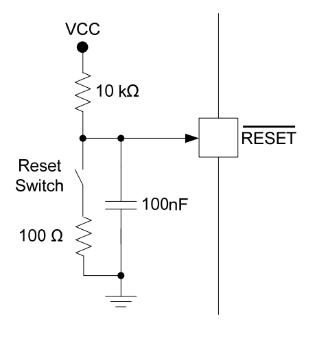
Although xmega's can be programmed through dfu mode (device firmware update), they don't ship with the bootloader, so I had to have
an AVRISP header. Though, in contrary with other 8-bit AVR's, xmega's use PDI interface to communicate. Moreover, the PDI_Clock pin is
shared with the (negative)RESET pin, which limits the choice of the capacitor I can use to decouple it. In an ATMEL's
Application note about the schematic of xmega's boards they propose the circuit on the right for the reset pin, but the capacitor
is inserted only after the dfu bootloader has been loaded. Worth noting is that even in the DFU mode operation you still have to use
the RESET pin to toggle between the DFU bootloader address space and the application space, if you don'y want to plug the device in and out.
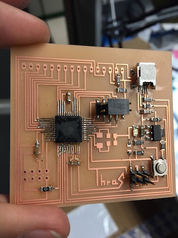
Moving on to the board routing was quite easy, after I put four 0 Ohm resistors to jump cables. The biggest hurdle was to minimize
the effective area of the board, so that I can house it directrly lower from the electrodes. As you can probably see in the photo, I have made
a design error that I discovered only much later on, when I plugged my board to the USB port. I am having traces running underneath the
the mini usb shield, inevitably touching it a shortcircuiting. Luckily, the cables where power and ground, so the operating system shut the
usb port very quickly, due to excess current flow, before any electronics was damaged.
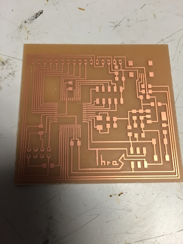
Milling the board proved to be hard, but after a few trial and errors I think I became a guru. For the most successful run (which you can see
here) I did the following steps:
1. Use the 1/32 inch end mill with -1 offset to clear most of the excess copper on the board.
2. Use the 1/64 inch end mill with 1 offset, to get to the places the bigger end mill couldn't.
3. Use GIMP to isolate the miniUSB and microcontroller pins and run the file with a 10 mil end mill, to get nice big pads. Be
careful with the isolation so that you don't accidentally cut some pin traces.
4. Use the 1/32 end mill to mill the through holes and cut the outline of the board.
Stuffing a board had become a routine process, yet this time it had some particular difficulties. I had to place a small insulating patch
underneath the miniUSB connector and then solder it on top. I used a small pieace of thin epoxy tape. In addition, as there was no
single layer pcb stock, I had to be very careful with anything that past through to the other side. I had to resolder the female pin headers
many times before I achieve an even height and no shorts on the back side. In the final iteration of the board, I used a thin layer of epoxy on the back side
to trap the tips of the header pins and insulate them from each other.
Having a stuffed board it was time for smoke testing and subsequently programming. In the first iteration of my board I spend
a considerable amount of time trying to debug the "USB device drawing too much current" issue, when I finally realized it was
the miniUSB shield in touch with ground and VCC traces. Apart from that everything looked fine, and the AVRISP recognized
immediately the device. I also burned quickly a USB DFU mode bootloader from Atmel, after which the device was
recognized by my Macbook as "Composite Device" and I was able to program it using dfu-programmer.
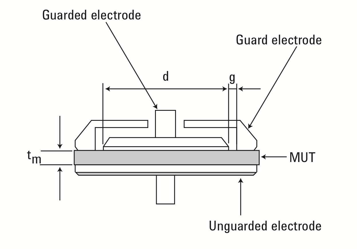
Step 2: Designing the electodes
For my electrodes, I chose the contacting parallel plate method, as it requires no material (MUT) preparation
and the operation involved when measuring is simple, while it gives precise results for low frequencies. I used 3 electrodes in my
design. At first, there is an unguarded electrode at the bottom. Then, on the top side I have a smaller electrode guarded by an outer
ring electrode. Thus, the electric field lines on the edge of the guarded electroded are "absorbed" by the guard one, which is connected
to ground, without affecting the measurement of the uniform, straight field lines in between the plates. The electrodes
are circullar as opposed to parallel for a more uniform distribution of the electric field lines.
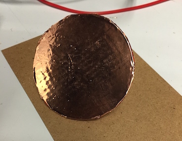
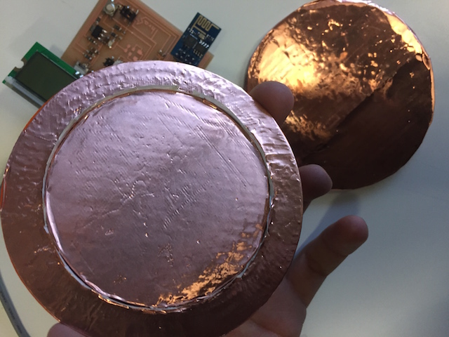
Prior to molding and casting the electrodes with the aluminum alloy, I decided to 3D print them in order to get a sense
of their dimensions and applicability. I used a Makerbot Replicator 2X, and the results where pretty good! The clearence between
the guard and guarded electrode was relatively small, but with a little bit of sanding everyting fit in place.
Due to shortage of time and resources arriving in time (I had ordered a special, low impedance aluminum alloy) I didn't get
to making the electrodes out of molding and caster. As I had already my 3D printed parts, I decided to copper coat them and create the electrodes
this way. I used copper tape and epoxy tape and cut pieces with the vinyl cutter to fit the 3D printed design. The end result looked pretty nice,
especially the guarded electrode which was press-fit with a layer of epoxy in the guard electrode, forming a very stable body. Running out of time,
and with my board unwilling to program successfully, I settled down with this pair of electrodes, until the end.
** CLICK on the image to see more pictures of the electrodes **
Step 3: Programming the MCU
Programming the xmega initially appeared straightforward. There were numerous Application notes from Atmel giving examples for
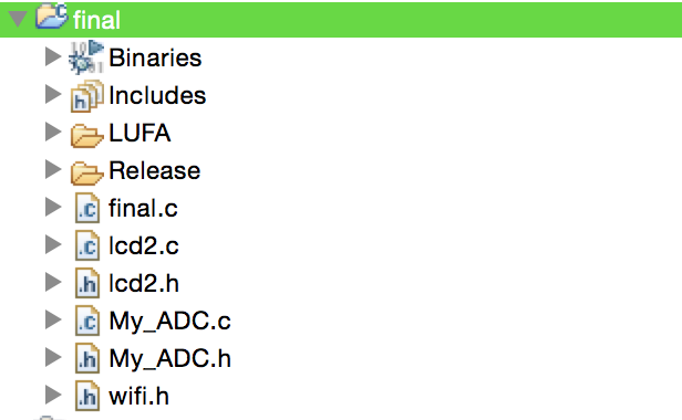
ADC functions and I was already familiar with programming the LCD screen and the WIFI module. I split my code into 4 files,
one for the LCD, one for the WIFI, one for ADC calibration and the main file. For the hardware serial of the XMEGA, I used the
peripherals part of the LUFA library. It was a hard time trying to build it through eclipse, as LUFA works mainly with its own
makefiles, but by tracing out the dependencies I managed to do it.
I will explain now some bits of the embedded code worth noting.
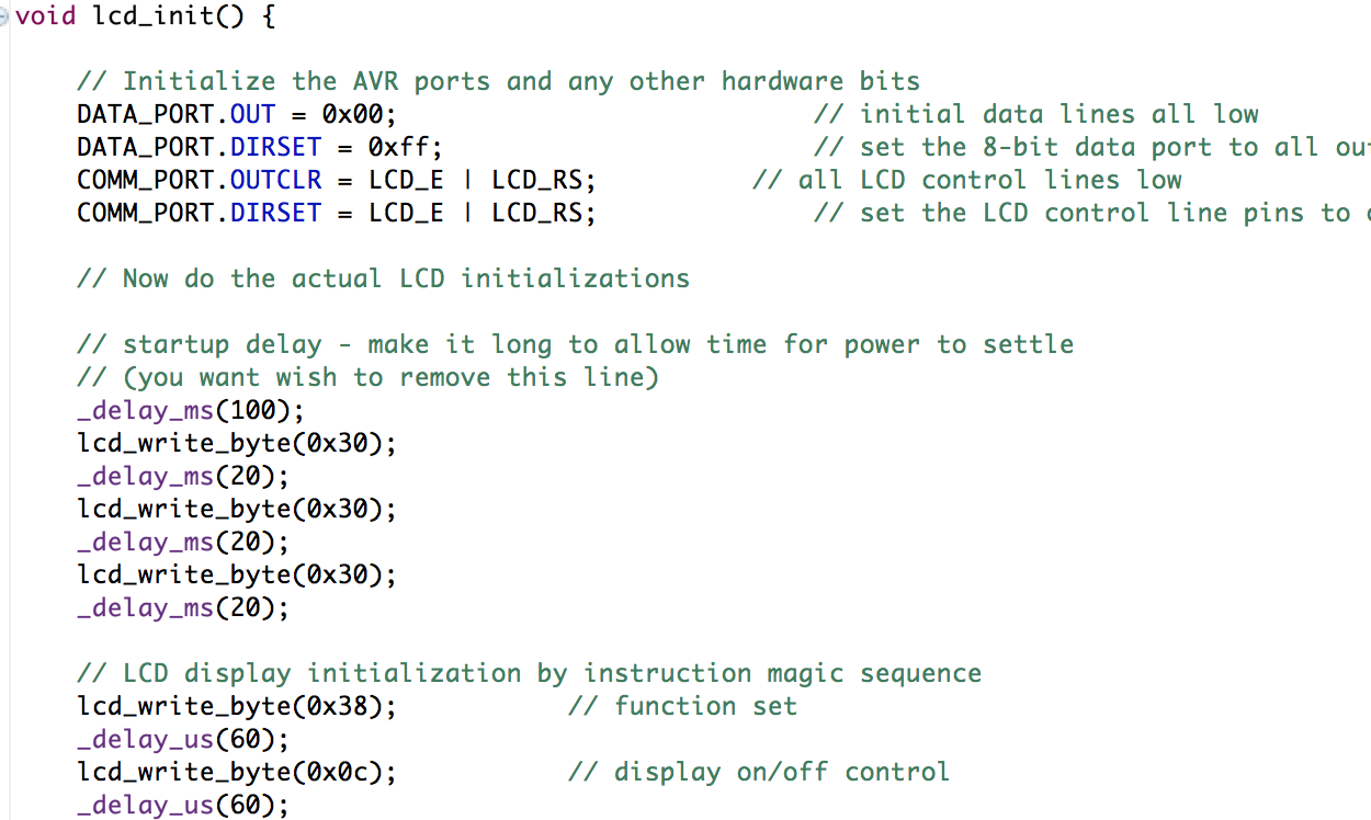
Here you can see the code snippet for the LCD screen. I changed the LCD library 3 times (Arduino's, 8051projects.com, mikroe.com)
because my LCD screen was not wowrking with
the xMEGA. In the end, I wrote my own initialization function because there was a huge discrepancy in the waiting times
between the commands in every library. To elaborate, to drive the LCD module you have to go through an initialization sequence,
with a series of 6 commands with different execution times. Thus, you have to send the commands with the correct timing (taken from the
datasheet of the LCD, which is very nicely explained here)
or else it won't start.
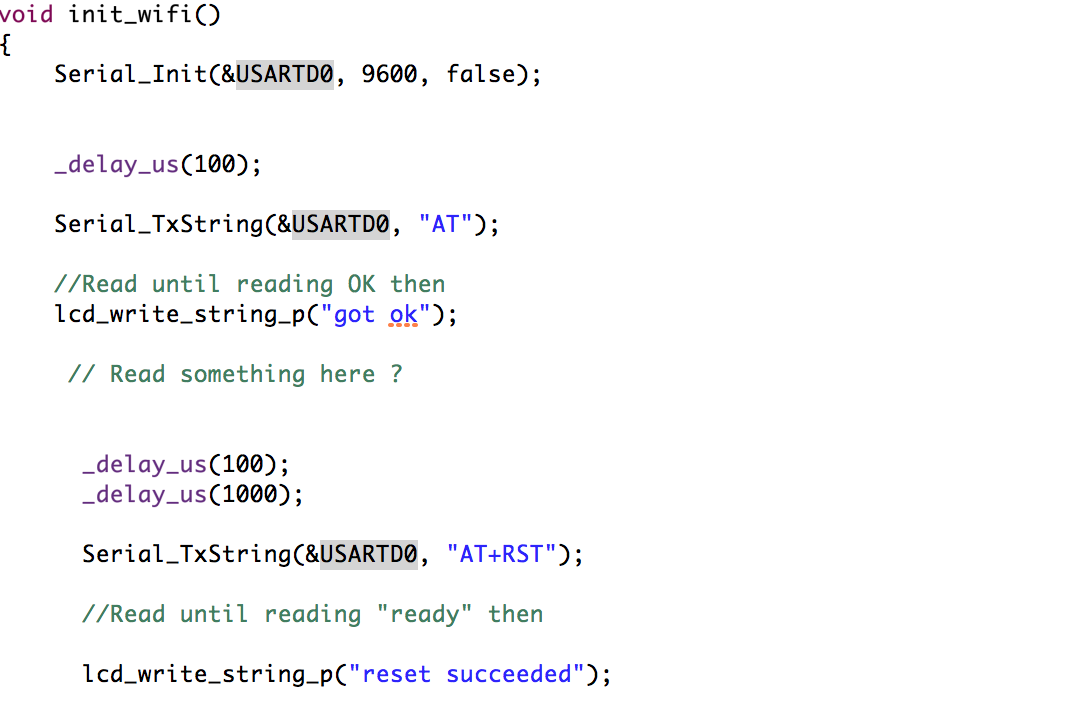
For the WIFI I used the same code I have written in Networks and communications week, but now I am sending the commands
using the Serial_XMEGA library from
LUFA.
At first I join the MIT Secure network and then I setup the wifi module as a web-client following this
tutorial. I will do GET/POST request to my
class website to get the ADC's raw data and then perform signal processing and the Fourier transform. I could also use the wifi module
as a web server, but the current it consumes to listen to requests might be prohibitive for USB power input (it can go around 300mA).
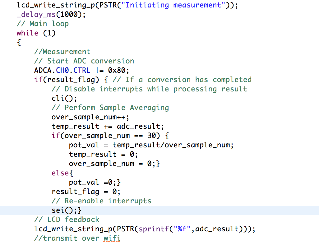
To program the ADC I read ATMEL's appnote about the XMEGA's ADC. Due to shortage of time, I didn't implement something more elaborate
than a simple oversampling and averaging, so that I at least could get a nice capacitance measurement. In order to get a good time
resolution, I have to send synchronous pulses and sample at different time intervals i.e. start the ADC conversion with different
delays. I can also try to perform a series of ADC conversions at maximum frequency (~2MSPS) and store the valuesin successive memory
addresses. I will experiment with different techniques in the next spiral.

