This weeks project is to design, mill and stuff a circuit board with an LED and a button. The goal is to learn to use circuit design software. As I was already familiar with the ORCAD design suite, I decided to try out EAGLE. It has a free version featuring a design of up to a 2-layer board, which will be more than enough for this week's project.
The user inteface is a bit tricky in the beginning but after a learning curve the software is powerful. The software has also a command line where you can write commands instead of clicking around, which proved to be very useful after the first hours working on it.
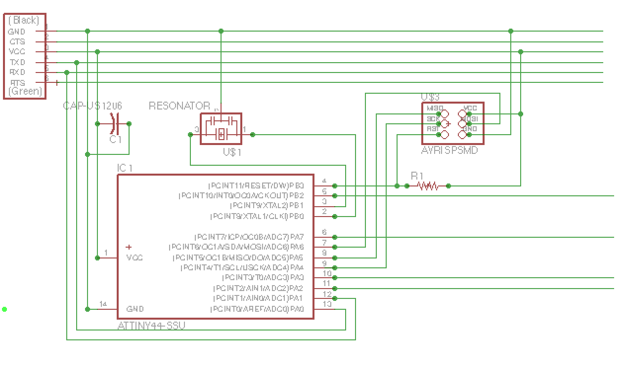
Step 1: The schematic.
On the right you can see my first attempt to wire the different components in the schematic. At that point, I have totally forgotten that you can give names to wires and couple them without actually routing them all the way, so I implemented a naive "horizontal bus" architecture, in which the different components are vertically oriented below the input bus line.
Yet, as you can see it becomes really complicated even with such a low number of components, thus the moment I realised I can name my wires, I moved on the second implementation.
Tip: Don't forget to use the Net tool instead of the Wire tool, as with the latter you are not actually connecting with the components. Think of the Wire tool as drawing lines of wires that can be later on connected with the Junction tool.
After using names and labels for the wiring, the schematic became much more clear and comprenhensible. I decided to create a visual "input/output" bus with the free ATtiny pins and Vcc/Ground, i.e. the elements available to any extra components I insert, like the LED and the button.
Here is a list of the components that I used. I inserted them from the fab library (download here).
1. ATTINY44-SSU : the microcontroller
2. 6-pin FTDI : for communication with the pc
3. AVRISPSMD : 6-pin jacket for intefacing with the programmer
4. 20MHz Resonator: to clock the circuit
5. R1206, C1206, LED1206 : Resistor, Capacitor and LED from the 1206 family for surface mount soldering
6. a 4-pin switch
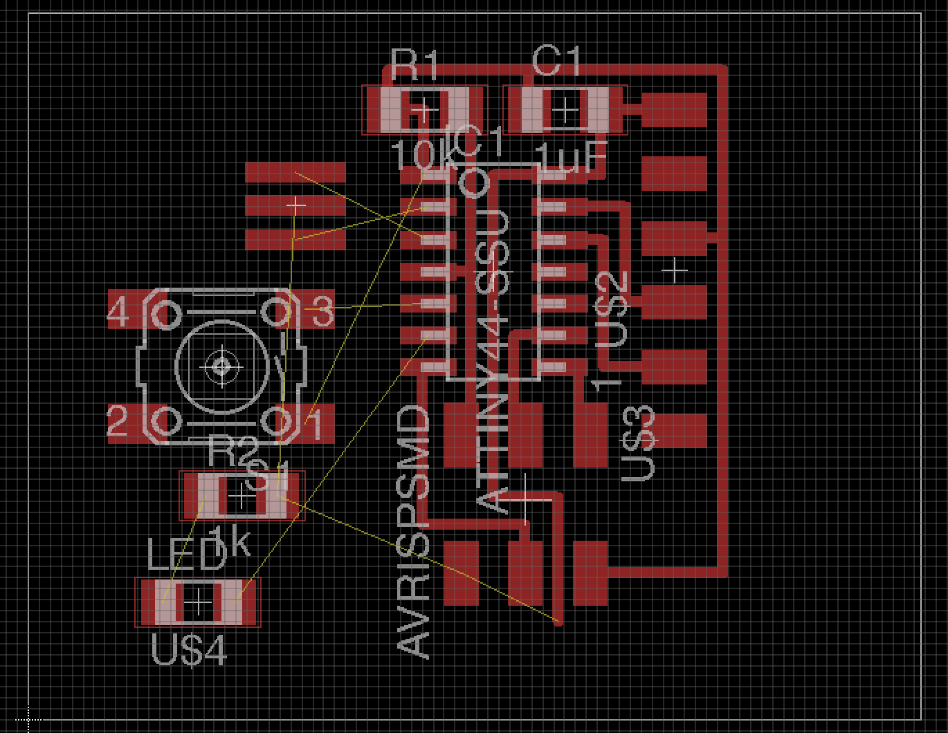
Step 2: Routing.
After I finished the schematic, I moved on to the board layout. Using the automated schematic-to-board function from EAGLE,
the components showed up in the board layout with yellow lines indicating where a routing should be made. Important: Before proceeding to moving components around, you should change the default grid size to be at least as fine as the end-mill you will use for the milling. I set mine to 16mils with an alt option of 1mil, which worked the best for perfect alignment of every component.
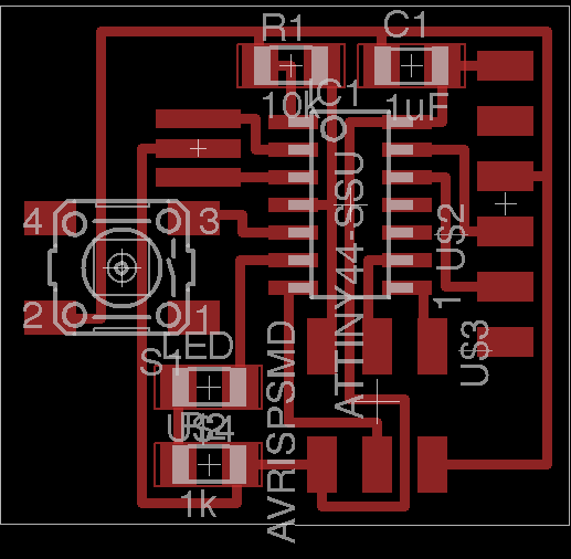
As you can see in the image, I followed the layout of the example hello.FTDI board for most of the components, as it was already optimized for them.
I placed the button and the LED/pull down resistor on the left side of the board, because the position of the resonator created a nice gap below it. After finishing the positioning of every component, I ran the design rules check to find out any inconsistencies in the gaps between the conducting parts, i.e. gaps smaller than the size of the endmill. By using the size of the endmill as the default grid size, the positioning had zero faults, as it was very easy to align the components using the grid as a measure.
The dimensions of the final board were: 1.2x1.5 inches, which is a nice size for the 1/64in endmill.
Step 3: Milling the board.
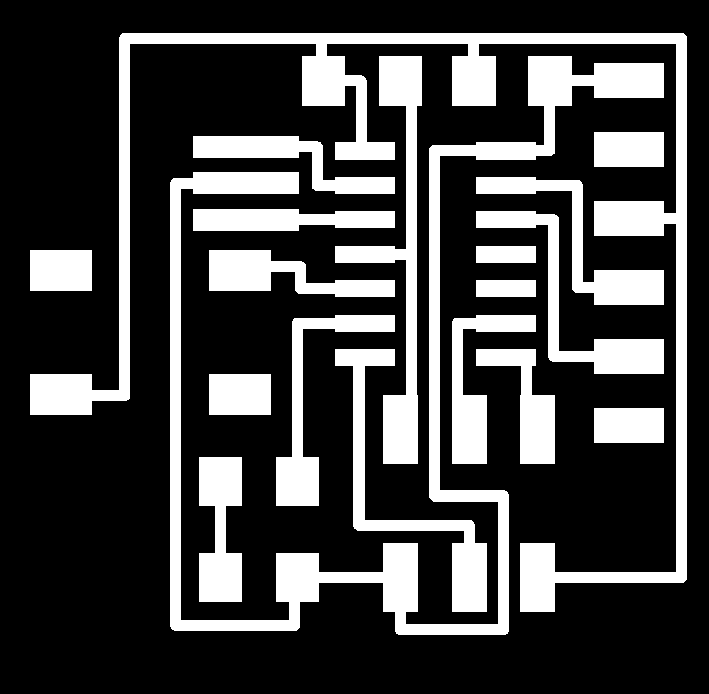
Having the board layout in place, I had to acquire the images for the toolpath generation. Again, using EAGLE it is straightforward to go from the layout design to an image from which the fab modules can generate a Modela toolpath. I displayed only the top layer (hint: write in the command line "display top") and exported a PNG image. Subsequently, I drew a frame around the board using on the bottom layer, and then by displaying only the latter I exported the aligned PNG image for the outline milling.
Like the 3rd week, I used the compiled fab modules (make_png_rml) to generate the toolpath. I tweaked the tool depth and followed exaclty the same milling procedure as described in week 3.
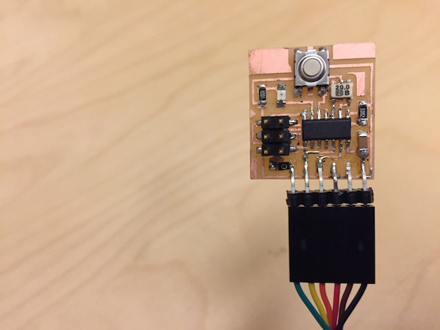
As you can see in the image, the result was good enough. I think that the endmill was fairly new, thus I had very fine finishing in the traces. I deburred my board using a steel ruler and cleaned it with soapy woter to remove any finger oils before soldering.
All in all, the workflow from EAGLE schematic to the milled board turned out to be very time-efficient and straightforward. I really enjoyed the simplicity of the whole process, and I think it's great to have such a low-cost and fast circuit prototyping procedure.
Step 4: Soldering the components.
This week the soldering was a total failure. I will try to summarize what went wrong in 3 steps.
1. Read carefully if you are using lead-free solder or not. The leaf-free solder is not happy in low temperatures and can be very frustrating if you cannot melt the huge solder-blob you created. After my experience with lead-free solder, even after I realized it and raised the temperature of the solder gun, I recommend strongly the use of the normal, leaded solder. It is much easier to manipulate it and has a better flow on the components' surfaces.
2. Be very, very, very careful when soldering the FTDI jack. It is very easy to solder with a slight upwards tilt, with result a total breakdown after you try to connect the cable. Needless to say that this happened to me, and I had to use a 0 Ohm resistor and some huge blobs of solder to save the board, as pieces of copper were ablated from the surface.
3. Be very, very, very careful when using a multi-meter to check your board when it's plugged in to a USB port. If at some point you short-circuit Vcc and ground, your USB port will not be very happy about it. Thankfully my Macbook has a high current protection system that disables the USB ports in the case of such shorts.
Extra: Programming the board.
Despite the soldering failures, I finally managed to have a working "Hello World" board. I programed it using the FabISP programmer. When you press the button, the Morse Code for S.O.S is transmitted with the LED. If you press it again, it stops. I will post a more thorough programming tutorial on the Embedded programming week.