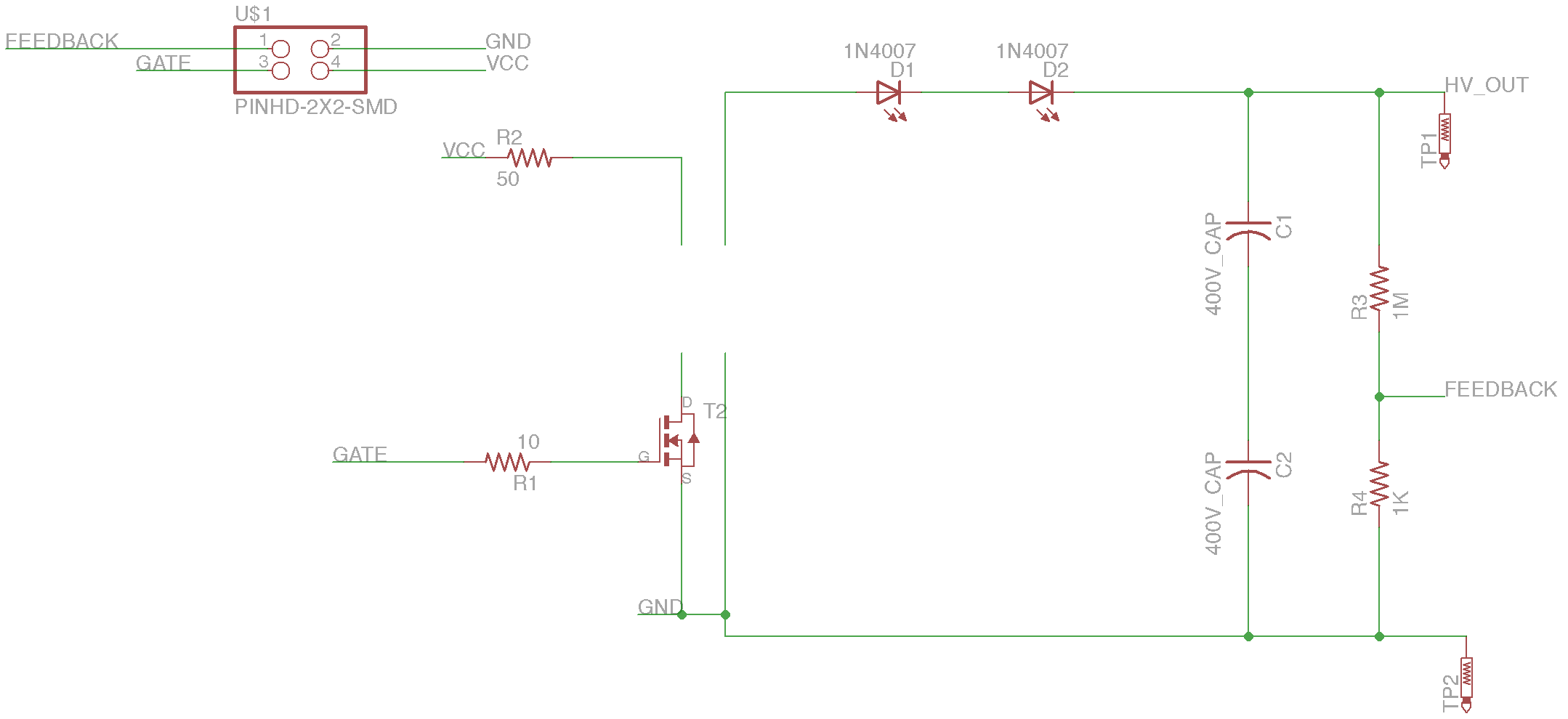
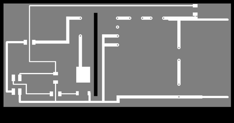
Schematic
In order to save resources, I decided to make this board a daughterboard of my existing microcontroller board from last week. As for the DC-DC converter, I first decided to go with a boost converter. I knew a bit about this topology before joining the class, so it was a good starting point. In short, it takes advantage of the fact that if you force current to stop flowing through an inductor, it will increase the voltage to arbitrary levels in order to keep that current flowing. By taking advantage of that arbitrarily high voltage, you can boost a DC voltage to a higher level. After reading around wikipedia and the general internet for a bit, I came to realize that while boost converters are quite good, they can only produce as much voltage as your switch will allow. In our case, the largest mosfet in the fab lab inventory can take 50V. I was looking to produce hundreds of volts, so this DC-DC converter topology wouldn't work. After some more reading, I came across the flyback converter topology, which is essentially a boost converter with the inductor replaced with a transformer. Since its using a transformer, you can have different amount of windings on either side, meaning you get voltage ratios between the two sides for a given waveform. 5V on one side might equal 100V on the other. I'm not doing a very good job explaining, but in short this lets you make hundreds of volts on the "high" side, and your switch on the low side will be subjected to much less voltage thanks to the wonderful voltage changing capabilities of transformers. I found a really helpful page fittingly called "Flyback Converters for Dummies", highly recommended to read if you're interested in this sort of thing. The image above shows my final schematic for a "fab" flyback converter. Notably the transformer is missing, as I don't know how to add parts to the fab Eagle library. I'll also note that the diodes 1N4007, and the capacitors rated at 400V aren't fab inventory parts. But, if you can get the parts, theoretically the "high" side of this could handle 500V or so. I have the capacitors in series to provide additional voltage capacity (at the cost of capacitance), and the diodes in series to provide additional reverse breakdown capacity. If you wanted to do the same thing but with fab inventory parts, you have to use a pretty ridiculous amount of didoes and capacitors.
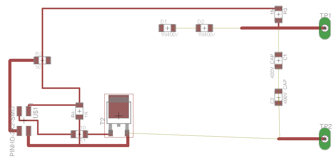
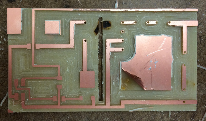
The board layout
The layout is quite simple, I was just trying to give things a lot of clearance for the high voltage aspects. Its about 1kV per cm for the breakdown of air with a spark, so without good clearances a high voltage circuit could easily discharge through the air. The diodes and capacitors are just placeholders.
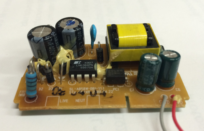
A external source of high voltage parts
So, I want to make a high voltage circuit, but the fab parts aren't up to the task. It turns out, you can actually get great high voltage parts in anything that has to deal with 120V wall power. This board in particular was from a cheap 5V power supply for charging cell-phones that I picked up in a junk bin. Just looking at the picture, I can point out some really interesting parts. Based on some head scratching, I was able to figure out more or less what was going on. In the image, the left side of the board deals with the high voltage AC and DC, whereas the right side of the board is low voltage DC at 5V. The board appears to take the high voltage AV, rectify it to DC (note the 4 diodes on the left hand side, classic full-wave bridge rectifier), and then switch it through a transformer with an integrated mosfet / oscillator / feedback chip (the LNK364). Interesting, this is the same topology as the flyback converter I described before, but downconverting voltage instead of upconverting it making the supply side the "high side" on the transformer. The small black chip to the right of the LNK364 appears to be an optocoupler for control loop feedback from the 5V side of the board. Anyway, for my purposes, the high voltage capacitors (4.7uF 400V), high voltage diodes (1N4007), and transformer were most interesting. Happily I was able to find a spec sheet for 1N4007 diodes, which indicated that this part was rated for 700V reverse breakdown.
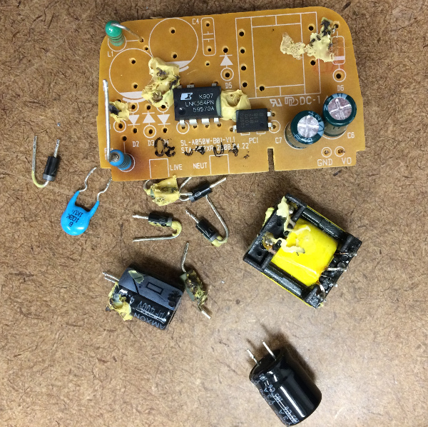
High voltage parts desoldered
I used the solder sucker and a soldering iron to desolder, and in the end got all the parts I wanted: diodes, capacitors, and a transformer. These parts are all through-hole parts, and without the know how to make custom Eagle library parts, integrating them into my design was very challenging.
Final modella milling mask
In order to use through-hole parts with my board, I had to measure them carefully with a caliper, design approximate parts in Inkscape, then overlay the parts onto my exported eagle .PNG. Additional traces were produced by overlaying white boxes. Honestly it took a long time, and I wish I knew how to do it the correct way in Eagle, but in short, it is very possible to mix and match SMD parts in Eagle and through-hole parts using some manual manipulation. I added a cutout in the middle, as this is pretty standard on high voltage boards. That being said, I've never actually designed one of these boards, or been properly taught at all. I'm just emulating the "good practices" that I know. Undoubtably this board breaks many conventions in high voltage design.
Modela milled
The modella milling for this board was the worst I've seen yet. Clearly the 1/32nd endmill was drilling deeper than it was supposed to, and in the multiple offsets of the endmill it left slights of boards between the passes, which makes me suspect I was using an older/smaller worn down endmill. Due to the high voltage clearance issue, I set the offets to 20 so it would mill out plenty of space. Unfortunately this means the milling took 50 minutes, which was quite inconvenient for my lab mates. Sorry guys! As you can see, even with 20 offsets there are a number of unused copper pads around. I used a somewhat unorthodox method to remove these pads. By heating the copper excessively with a soldering iron, you melt/burn the adhesive underneath. Through a combination of heating, burning, peeling, and patience, I removed all the extraneous copper.
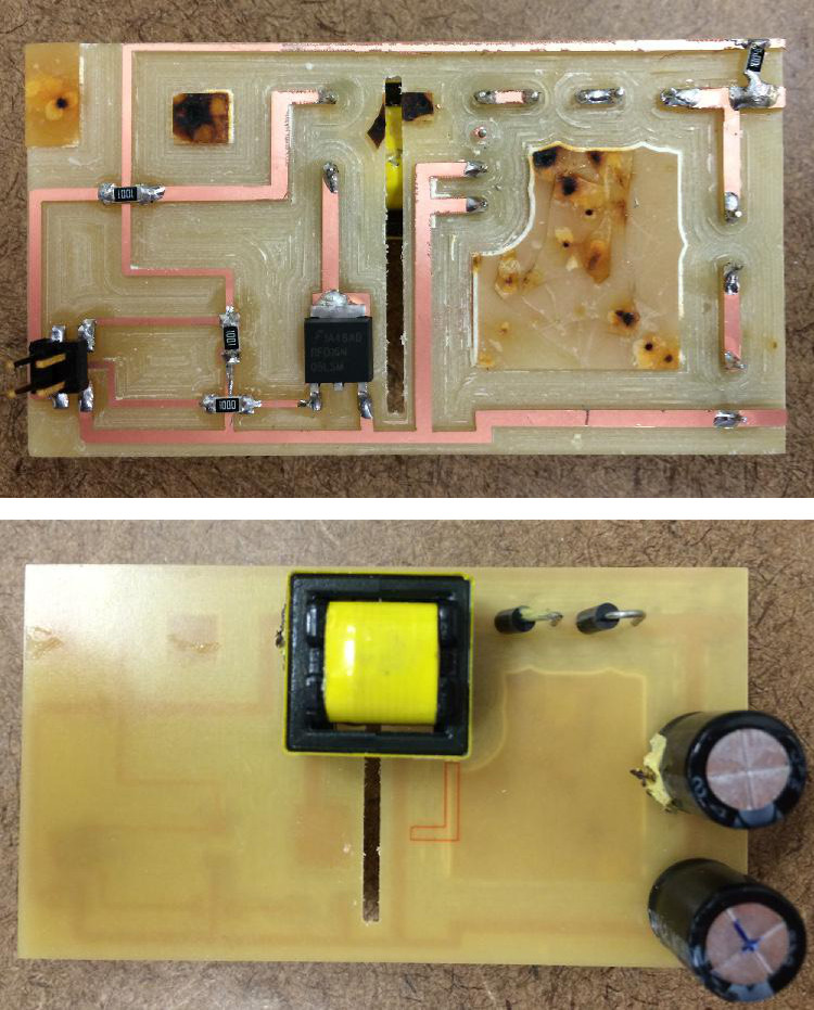
Soldered board - Top and bottom sides
It's not pretty, but it gets the job done. SMD and through-hole parts successfully mixed.
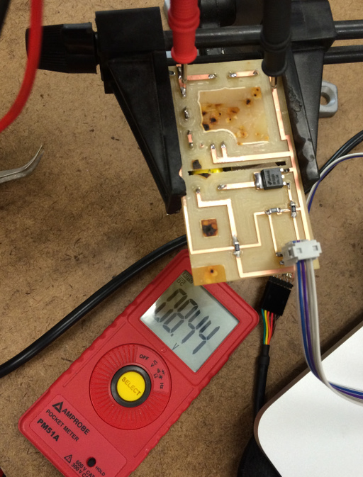
Test setup: Measuring the rails with a multimeter
But does it boost voltages? Here I show the test setup. The microcontroller is toggling the gate of the mosfet in an open control loop, while I measure DC voltage across the "high voltage" rails. This was after much optimization of the mosfet switching frequency and duty cycle, making current limiting resistors as small as possible, and also disconnecting the 1M feedback resistor. Even with all that I only saw a stable 8.4V with the multimeter. Without the leads from the multimeter, the voltage would climb even higher. Yes this is technically boosted voltage as it is above 5V, but it is much, much lower than I expected and wanted.
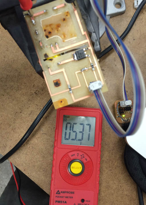
0.3V above the 5V voltage rail, not even LED worthy.
With the feedback resistor re-attached, the stable voltage falls to 5.3V. Perhaps the most worst DC-DC converter ever designed? Will have to reconsider making the high-voltage supply for the final project. But, since the feedback loop is setup, it might actually be possible to have the microcontroller emperically test a bunch of switching frequencies and duty cycles. Perhaps I'm not quite at the sweet spot.