Hello World ! Echo Board
05. Electronics Design
After understanding the basics of producing a PCB (milling it and populating it), it was time now to learn ho to design it. The goal is to use schematics to draw the board, then to mill it and finally to stuff it. The board to design will be used later on to actually run our "smart" system. The basic design is as follows (thanks Pip for this picture)
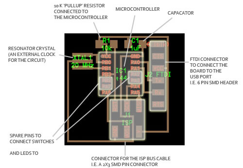
If we quickly go through the different components:
- Microcontroller: controls the parts on the board and is programmed from the computer
- "Pull-up Resistor:" this is a 10K resistor to keep the power into the microcontroller steady near VCC or zero (this is connected to the VCC pin)
- Resonance Crystal: This is an external clock for the circuit (this need the input traces to be connected to two pins on the board and the ground trace to the GND circuit). A Resonator is basically a Crystal with two capacitor in paralell to filter the signal.
- SMD Bus Connector: Takes in information from the FabISP and connects it to certain pins on the Microcontroller to program the board. (This needs to be connected to VCC and GND on the respective pins on the Microcontroller, and the other pins to be connected to free input and output pins)
- FTDI Connector: Connects the circuit to the computer to read in the program and power the board (this needs the VCC and GND pins to be connected to the respective VCC and GND circuits on the board, and TX and Rx pins to be connected to two free pins on the controller)
I actually wanted to implement two other components in the board, in order to "test" it: a switch and a LED. I needed to recall the basics of electricity (Kirchoff's laws, different components behavior) to do so. A good tutorial can be found here
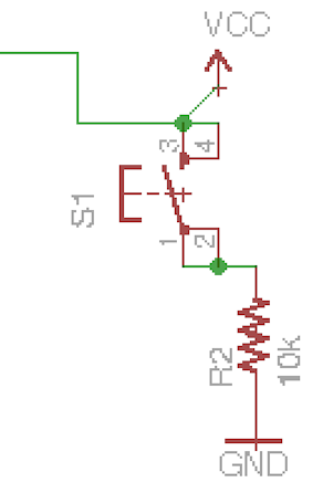
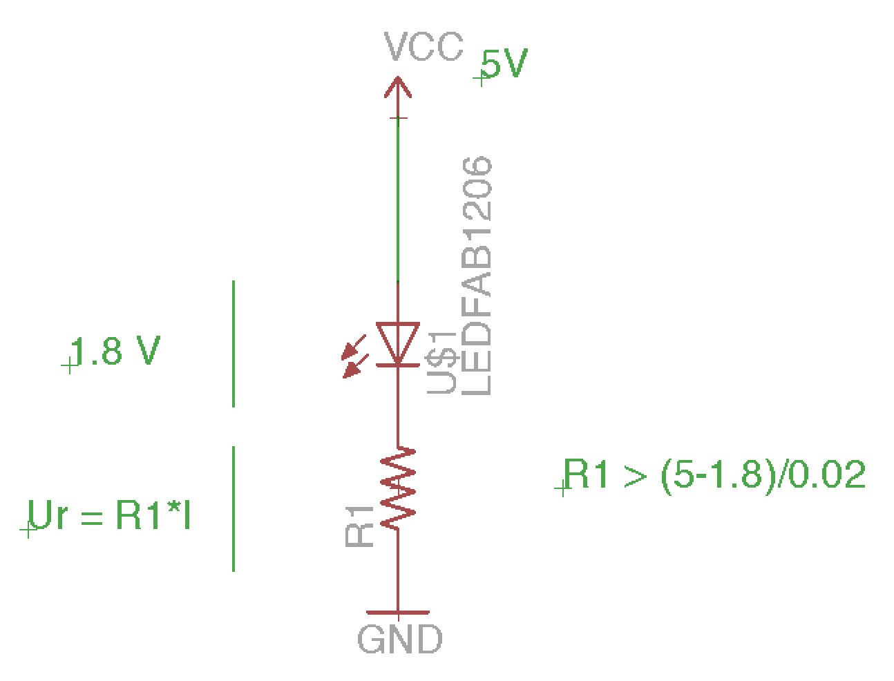
First, the switch: we want to be an input of the microcontroller so when we press the switch the microcontroller "feels" so current coming. So we need to start with VCC, then to add a pull-up resistor to it (otherwise it will burn the circuit. So the choice of the resistance was a 10k Ohms. Now, the LED is a little trickier. We don't want to add a VCC because it is the microcontroller that will send a current when he "feels" some current on the switch input. But we also want to add a resistor because other it will burn the circuit. The question is what resistor do we want to add? The characteristic of a LED is described as follows:
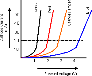
Despite the colors of the LED, we see that the characteristics, the LED acts as almost a wire for a voltage higher than some threshold. The theshold for our LED was 1.8 V. It thus lead us to a calculus of the minimum resistor not to create short-circuit.
The next step, to start designing the board, is to actually download a schematic software. The most common one is Eagle. A nice tutorial explaining how to download and install Eagle with the Sparkfun libraries can be found here. In addition to downloading the Sparkfun librairies, it is also interesting to download the fablab libraries, and to save the textfile as a ".lbr", in the Eagle library folder. We are now ready to go to start the schematics design.
The first step is to choose the different component and to place them in the schematic map. To choose the component, I looked at previous years, and picked components from the fablab with "FAB" in their name. I could usually choose the value of the resistors for example, even if it does not totally matter in Eagle at this point. A clear and nice website to guide you through Eagle can be seen here .
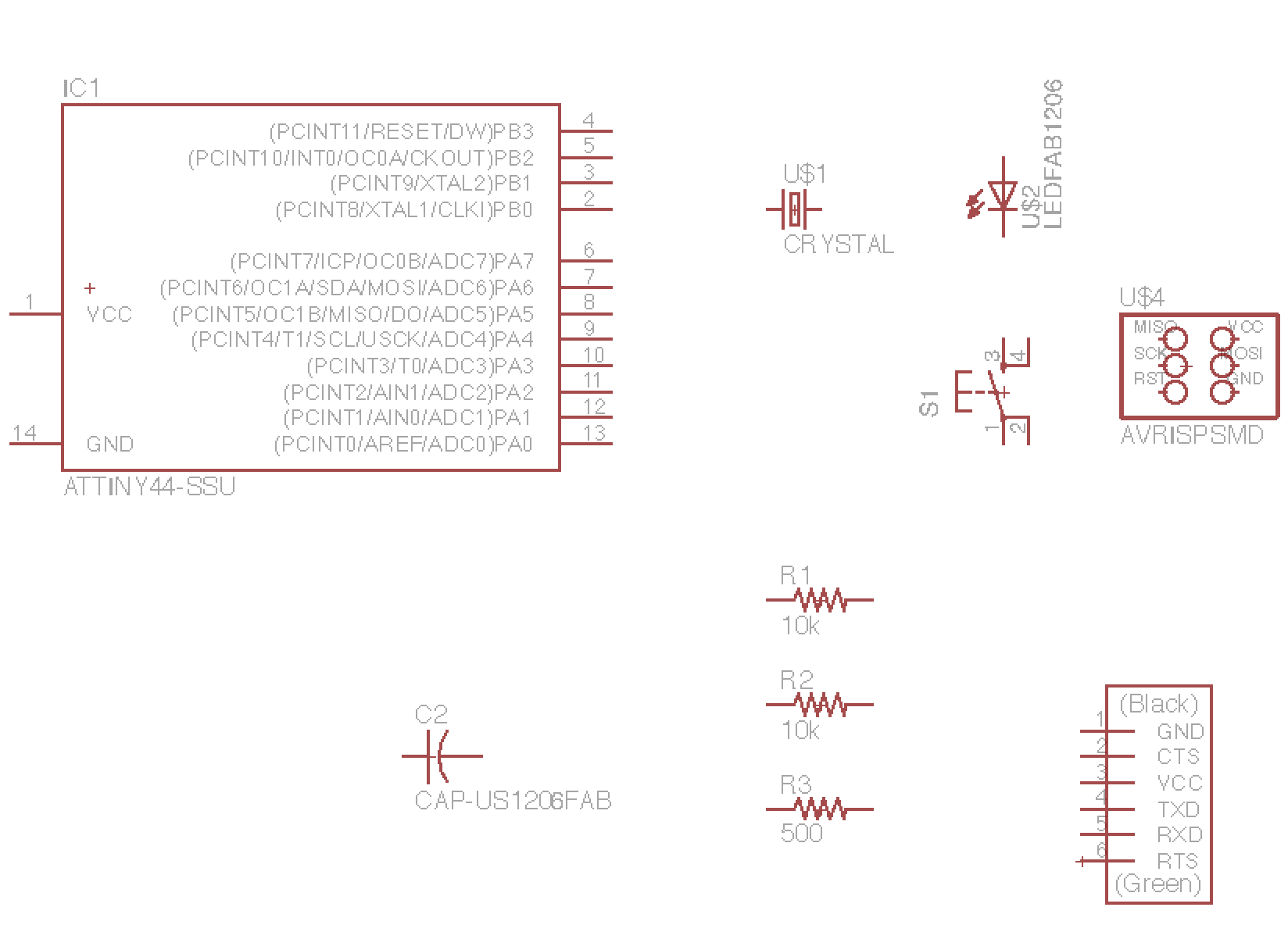
Once we have all the components of the board, we can actually drawing wires between them, using symbols such as VCC and GND, as well as Junction to make sure the wires are joined together, to clarify the schematics. Once it is done, we click on the layout button at the top of Eagle window and we can thus open the layout version of the board.
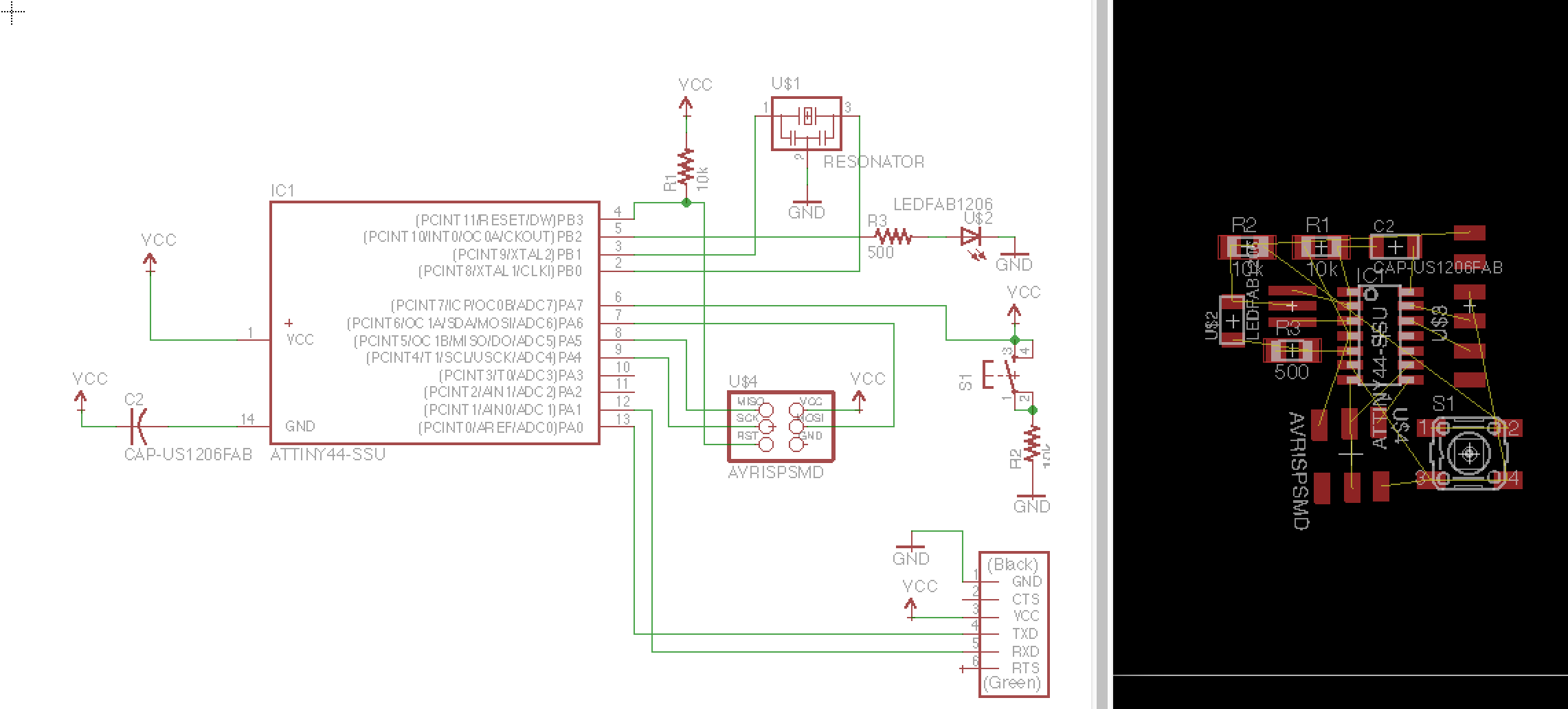
The line that we should draw are indicated in yellow and it is very intuitive. However, it is not obvious at all to draw teh connections without overlap and without too many "jumpers", to allow some wires to go underneath the resistor. A first good option is to turn and move the different components to make sure there is the minimum amount of yellow wires that overlap. And then try. You will quickly see that some connections are trickier and once you target them first, then it is easier. An option that can be interesting is to run the Autorouter option. With this type of baord it should not be a huge advantage but for more complex boards it is. I tried it but finally made my own. At the beginning, I had to have 3 jumpers and finally I succeed to have only 1 ! A useful tool is to check the errors we have. Some errors are useful to etect but other are due to the fact that Eagle does not see the jumper as a connection (because I did not wire it in the schematics), so can be ignored.
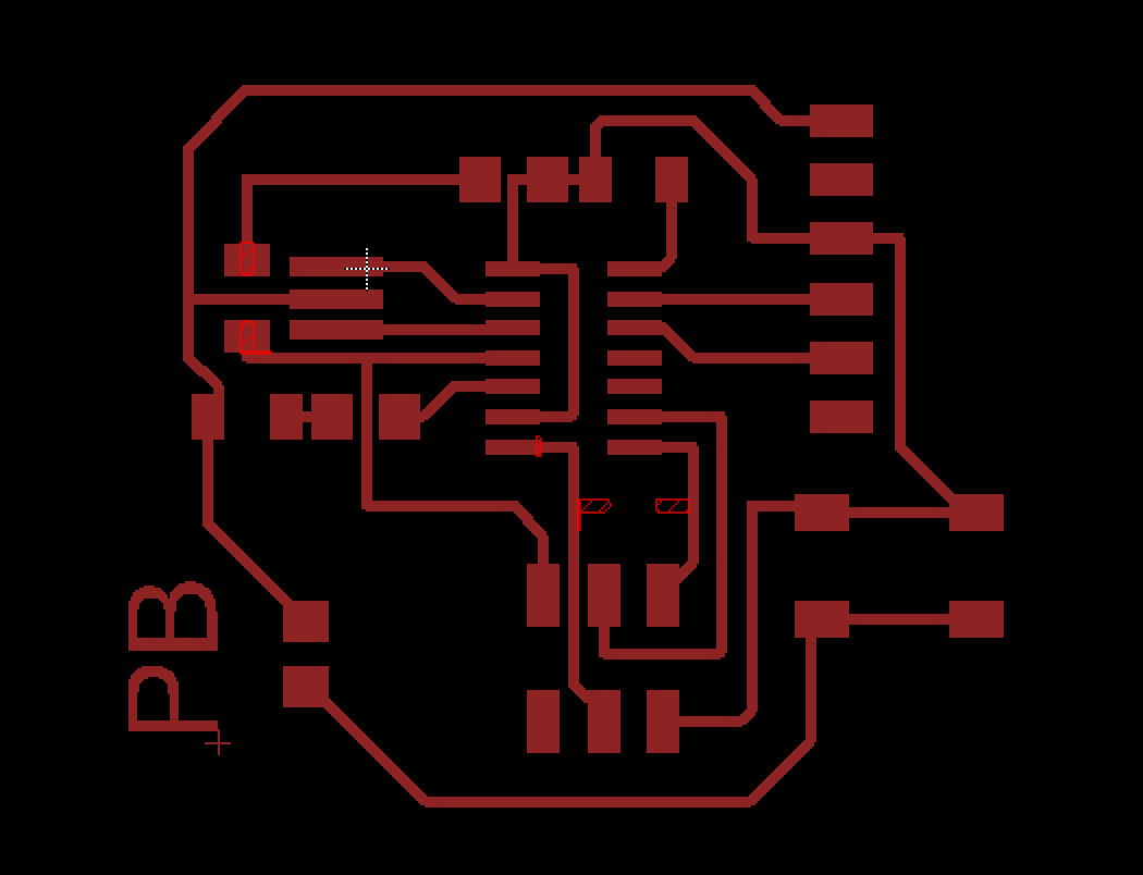
Once, I was done with the design, it is time to export it. First, we want to create a "milling" layer (number 46): a rectangle a little bit bigger than the traces, but a little smaller than the white delimitation, that should be shrinked around the traces. Once, this step as been done, we export the traces and the board. To export, we select only the layer of interest, we click Menu, Export, PNG. Then we choose Monochrome and a Resolution of 600. We do the same for the board (milling layer) and for the traces (layer #1). The output should be this:
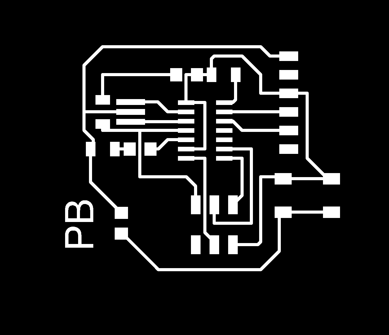
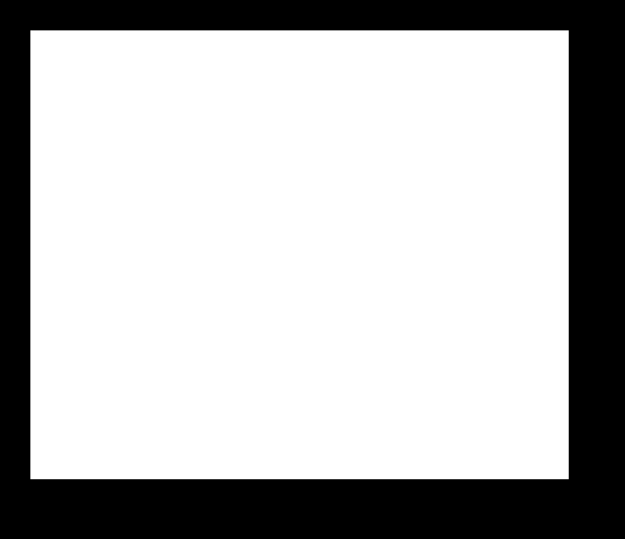
Now, the next step is to mill, with the Roland Mill machine using 1/64 mill ends for the traces, and 1/32 for the board. More information on this process here. At this point, I encountered two issues:
The actual file that I first exported was not only with the traces but also with the yellow connections that helps you retracing the traces. As I added a jumper, I did not have to use them so there where still there, and the design looked like that
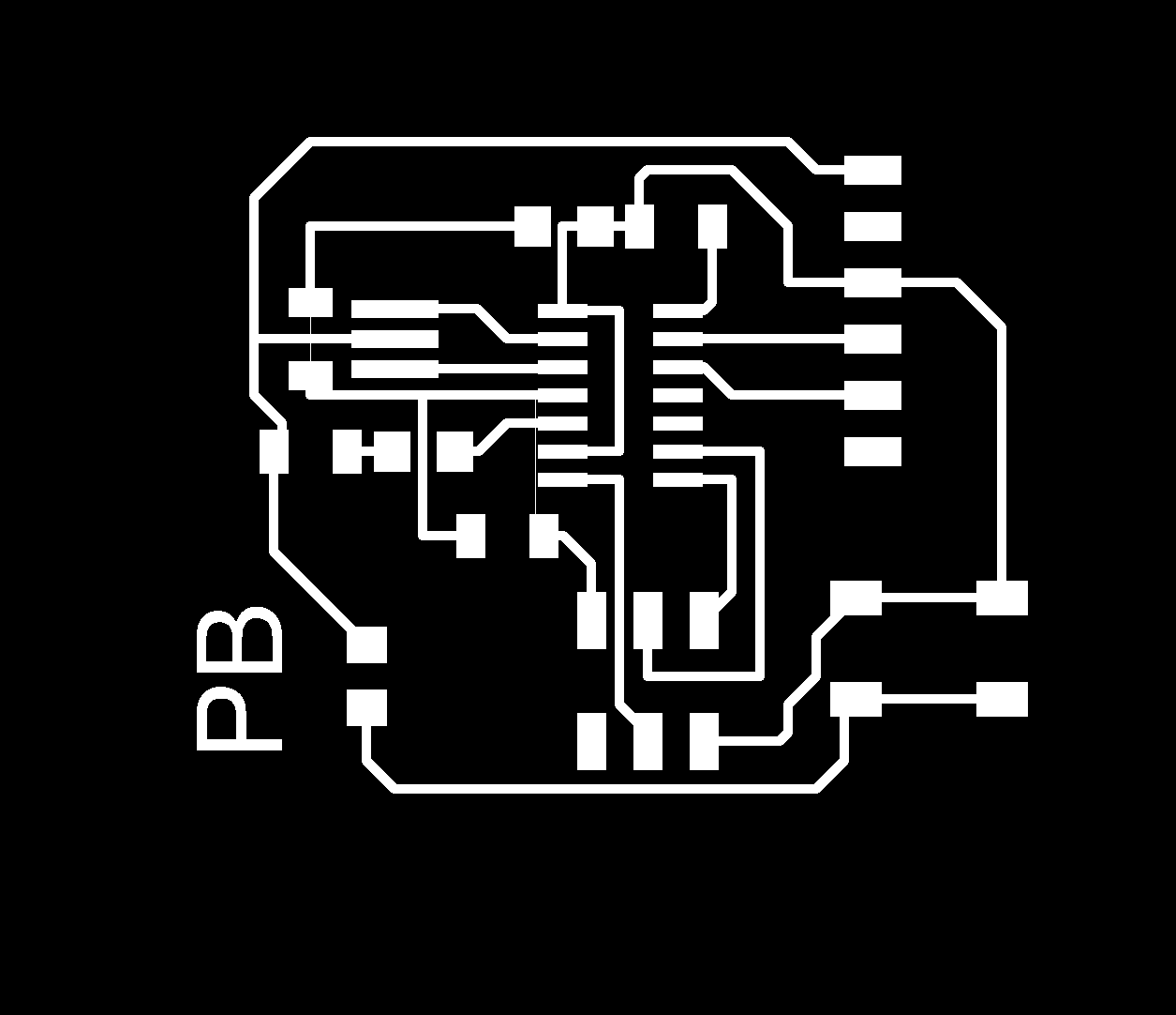
You can actually see these yellow traces. When I milled it, they were still there so I had to remove them manually (not ideal). I thus printed two boards. The other issue I encountered is that the sacrificial layer of the board was not perfectly flat so I had an inequal milling and I thus needed to increase the depth (from 0.12 to 0.25). Another issue I ran into, is that some of the traces were to close to each others (for the jumper and the 10k pull up resistor, so I had to manually remove the copper, that is never great). You can actually check the traces in fab module and predict that issue. You can also check the error editor in eagle
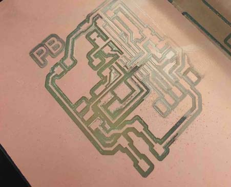
Once it was milled, we used the same techniques than before to populate it, and we had the following result
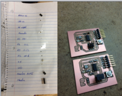
A tricky part was to figure out the good direction of the LED. It is written in the specs, but here is a good website to better understand.
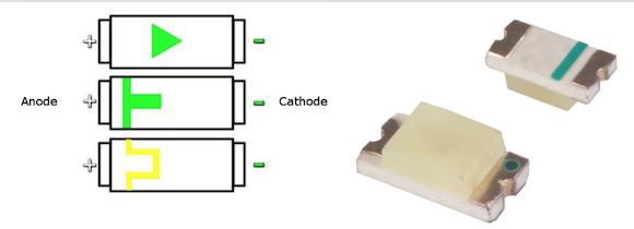
The next step was then to program it, as well as to simulate it.
To program it, I first download the Arduino platform to code, and I had to add the ATtiny library, following the instructions of this website. I then tried to write a code (inspired by previous other codes) in it.
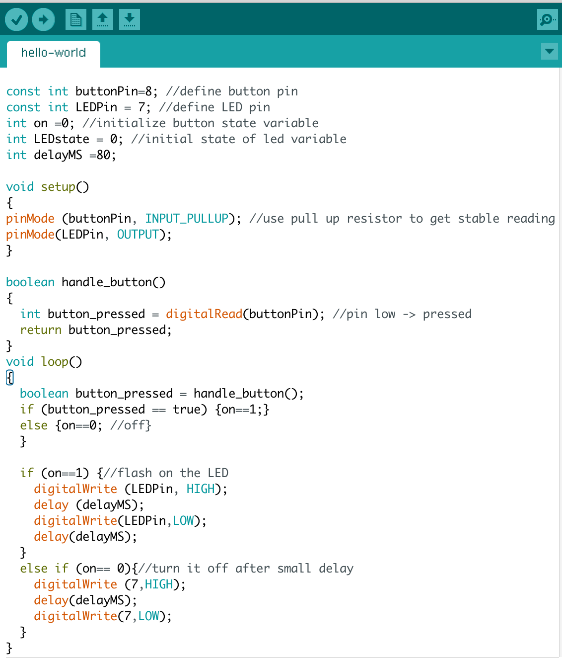
I then needed to plug the 2x3 pin of my ISP board to this new board, and to send the program through the ISP programmer, powering my new board with the FTDI connector.
I also wanted to simulate my board, using LTSpice. BUt I need to put more work on it.