Electronics Production
This weeks assignment is to create our first PCB (Programmable Circuit Board) and I am excited. The process seems pretty straight forward as we are given all the materials to create the board and do not have to design it ourselves (yet.)
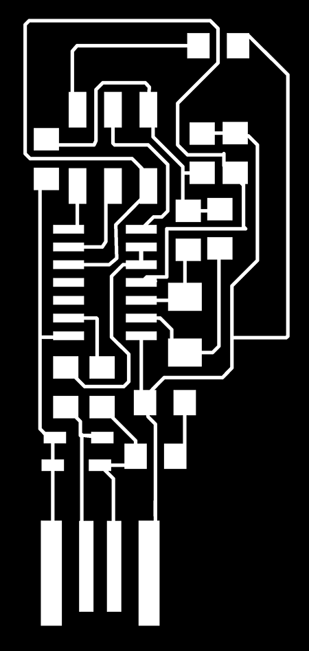
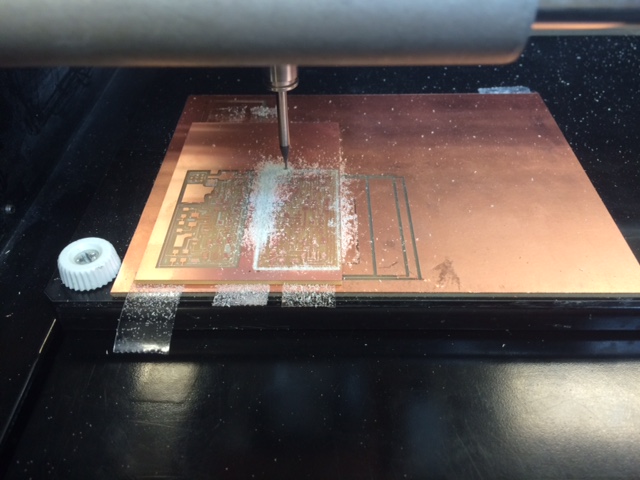
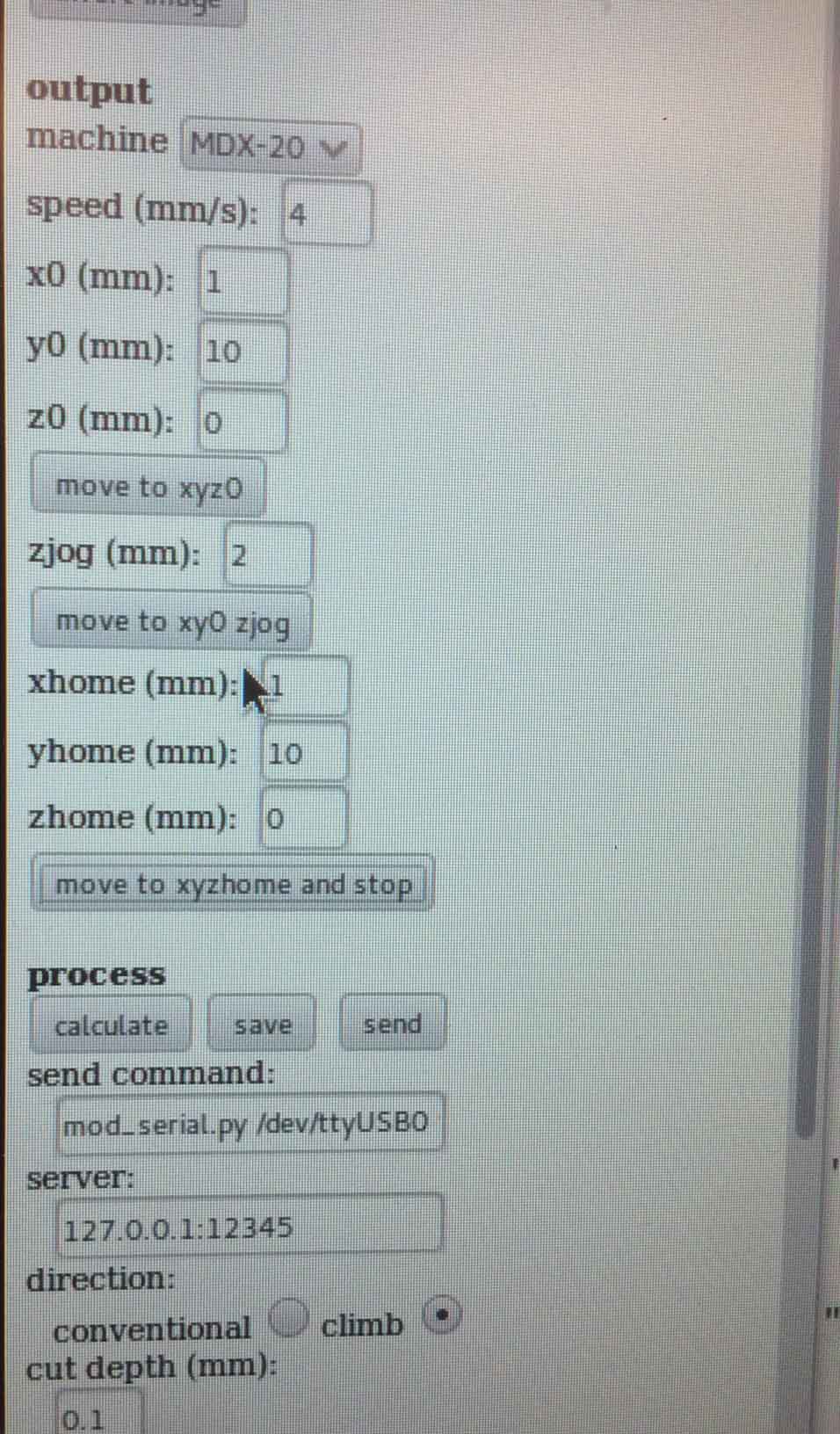
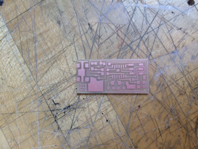
First step is to take the traces PNG into the fab modules. This allows you to send it to the roland mill to cut the traces on a copper board. One of the default things that I believe should be changed is cut depth. I make the cut depth .12 instead of .1 for a more consistent cut through than I have gotten using .1 as somtimes it will not go all the way through, however that could very well relate to the base plate needing to be replaced.
Milling Process:
Recommended: Change the cut depth from .1 to .12 for a more consistent and seemingly cleaner cut.
The next process is soldering which I feel pretty comfortable with because of some past projects. The process took about 20-30 minutes and I believe all of the connections are pretty clean. The next step is to attempt to program it. This will allow the piece to become its own ISP however I have to desolder a jumper after I program the board.
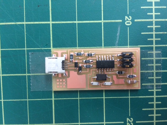
After a quick programming process that is layed out in the tutorials and was printed and give to us, my ISP is recognized by my computer!
