Electronics Design
Blink Board
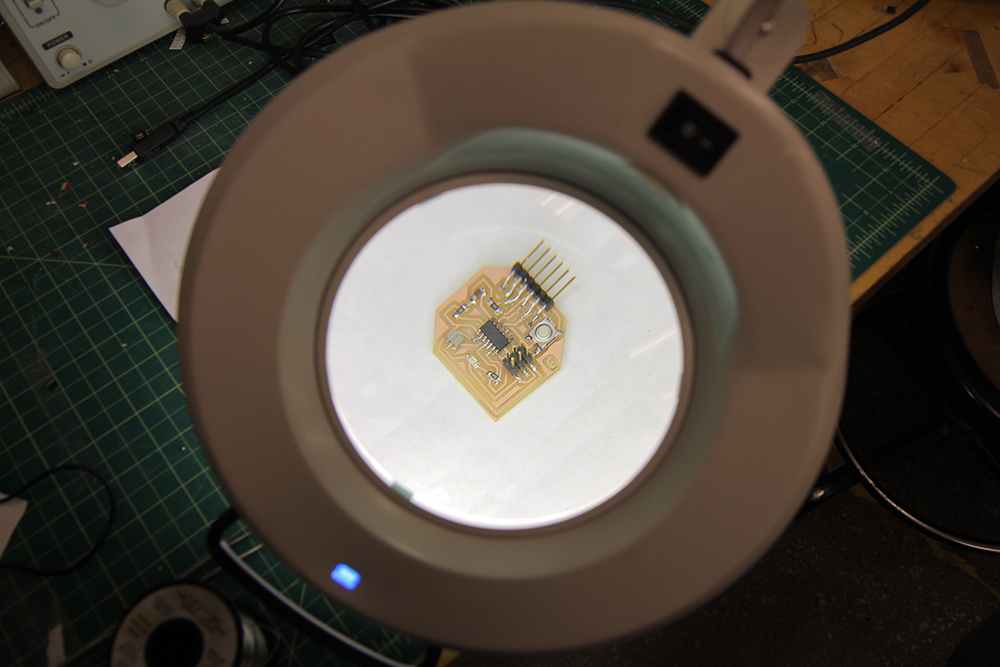
This week was hard. I get a second-hand of the book: Art of Electronics. Skimmed through chapters, introduced myself to Kirchoff's laws,learning the mechanisms of MOSFET's, diodes, LED's, op-amp's. Jeff's and Palash's recitation was also helpful. As soon as I felt a little comfort to start making things, I opened the Eagle software.
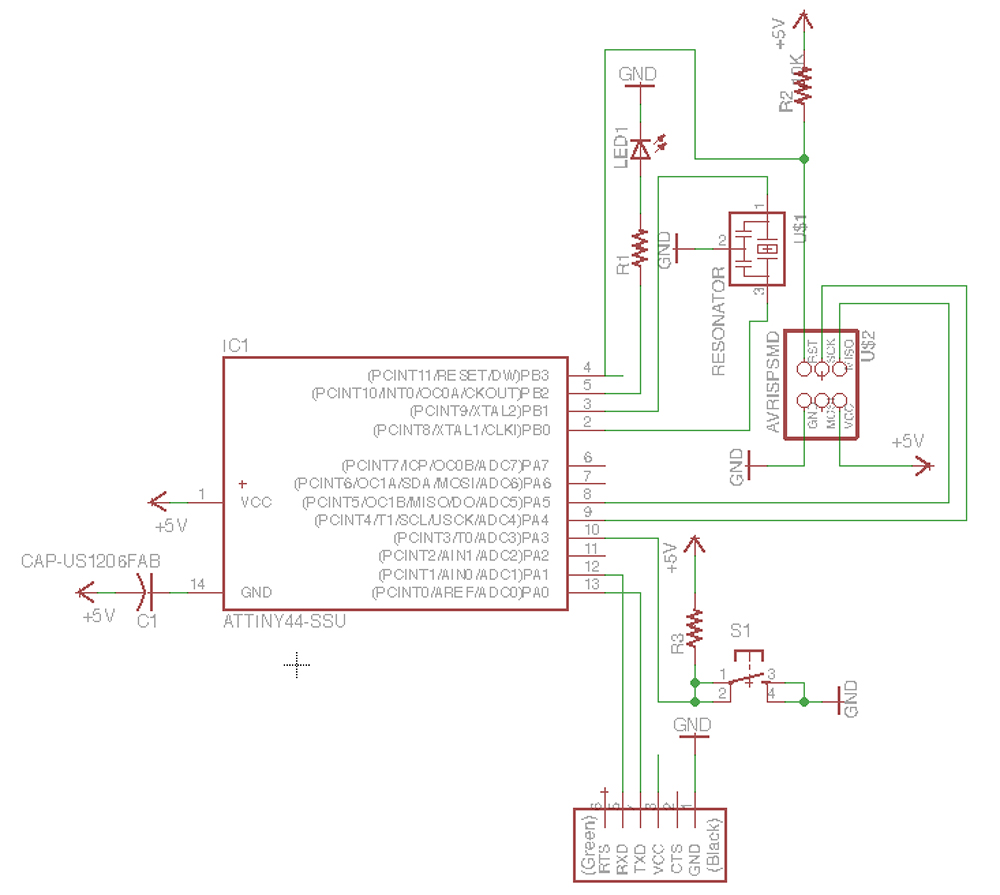
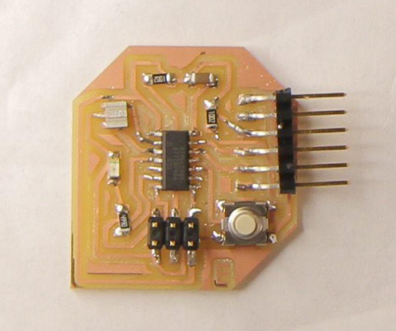
Decided to make a simple LED blink board. After downloading and installing the fab libraries and design rules, I worked on the following parts:
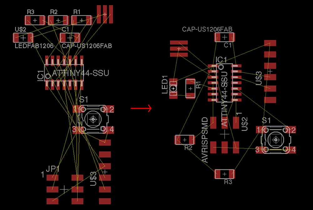
Whenever you decide to switch to board view in order to design the actual traces of your PCB, you will get a messy bundle shown in the top left. You have to arrange them spatially to produce routes between them. This part may take time, relax and listen something while doing that. 'Rotate' or translate the parts, Eagle built-in operations highlight the parts while you rearrange your parts, use them to produce better designs. Even I'm told that it's not a good idea to 'Autoroute', you may use it to get an idea about a possible arrangement of a final design. You may get rid of your specific routes by clicking on them using 'Ripup' command. Don't forget to make sure that your route widths are 0.016 inches. Although if necessary you may use a 0.012-in line especially for the ones passing under the microprocessor. But as I will show you in the following examples, there are other solutions for this kind of problems.
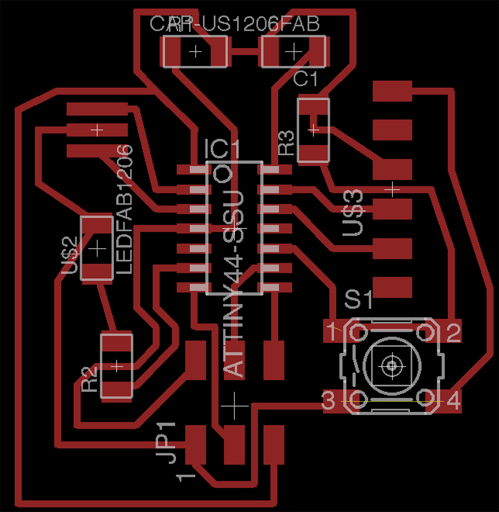
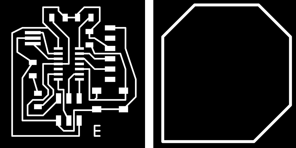
Don't forget the work on a specific layer, for example 'Top' layer for traces and 'Dimension for outline. Draw an outline with a 0.032-in width line:
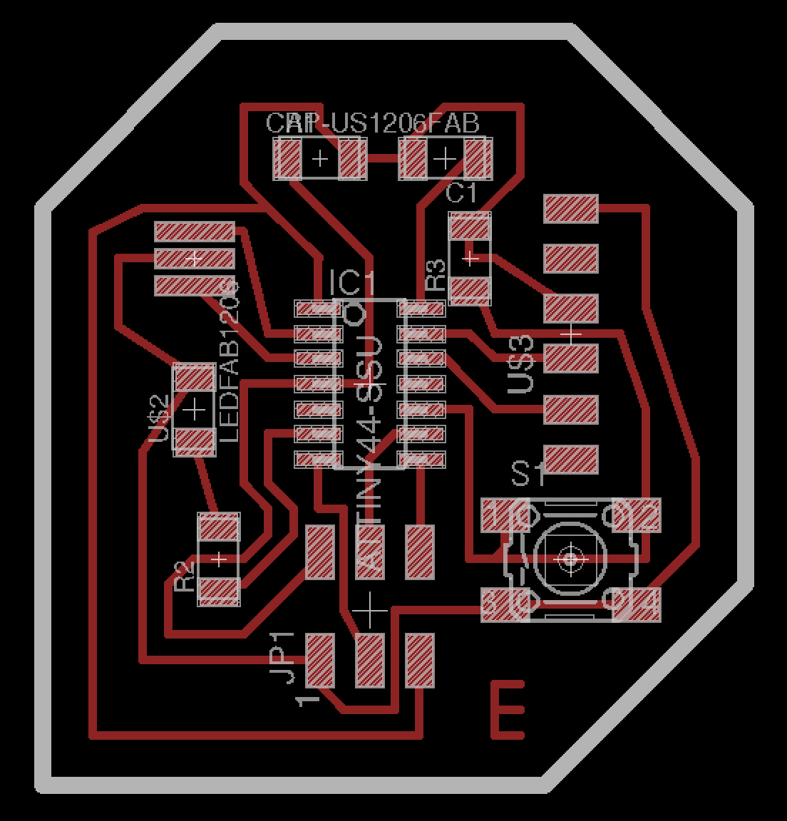
and you're ready to export your design as a png file, choose monochrome:
