Electronics Design
This week we were redrawing the echo hello world board and adding at least a button and a LED.
I think I played with eagle once a long time ago, so I figured I should give it another try at first for this project.
This week we were redrawing the echo hello world board and adding at least a button and a LED.
I think I played with eagle once a long time ago, so I figured I should give it another try at first for this project.

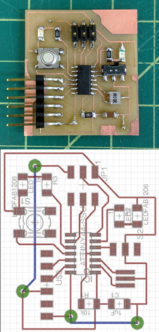
The schematic was fairly easy to construct based on the echo hello world board diagram. An important feature of Eagle is that you can name networks so you don't need a mess of wires running around the page. For my first board I added both of the buttons we have access to and 2 leds.

I added two jumper resistors to the schematic so that my traces could be laid out without crossing. These jumpers were added by figuring out where I would need a jumper to make my PCB work and then going back to the schematic and adding a 0 ohm resistor in the appropriate place. The Eagle FAB library has 1206 resistor footprints that allow a trace to be drawn between them. The top right and far left resistors are jumpers.
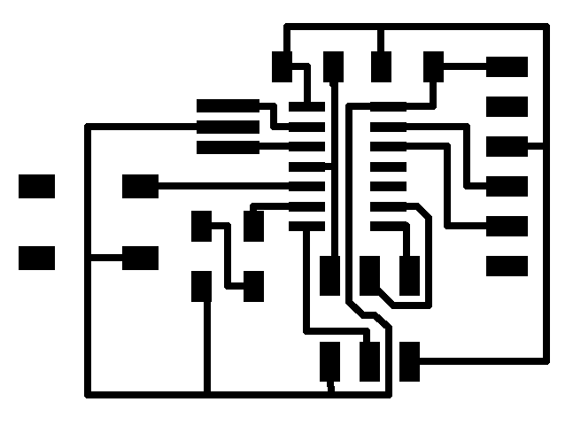
I also did a layout with just a single button and LED. Copying the layout of the example board leaves the spacing that we needed for adding the components, and means we don't need any jumper resistors.
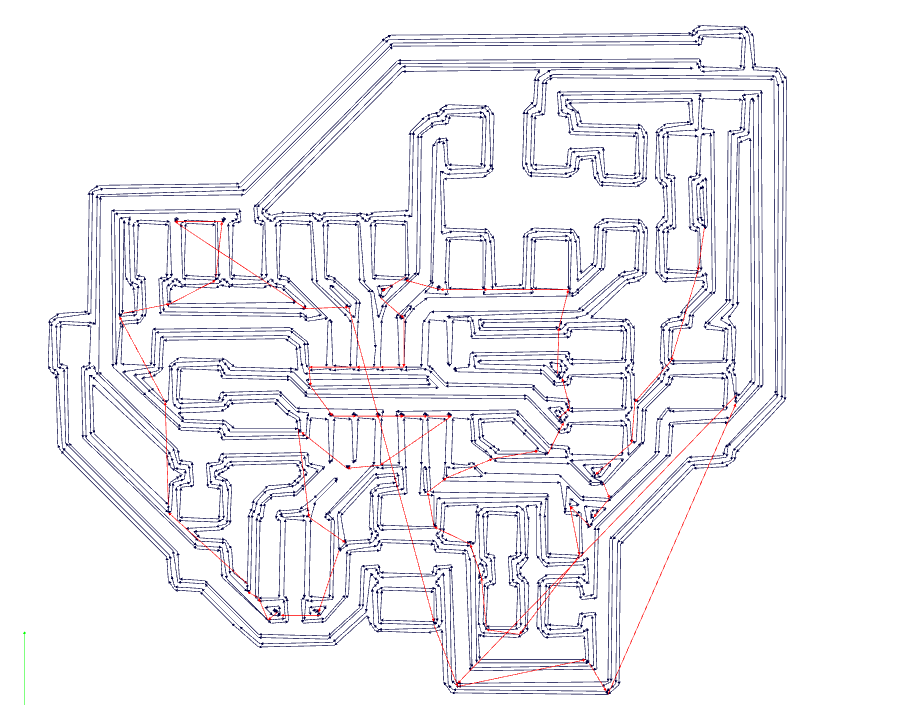
It is important to remember that the fabmodules wants to keep the white in your images, so it may be necessary to invert them. Milling both of these boards resulted in some slight issues where even though they passed the Eagle DRC with a clearence set to 17mil, there were some sections that were not fully milled. You can see that in the leftmost pins on both the top and bottom of the attiny44 pads in the toolpath.

These incomplete milling jobs can be fixed with a razor blade and some patience as you compare the schematic with the final product. I used 16 mil traces when designing this board. In the future I would use 10 mil traces to provide more room for clearence and reduce issues such as this.
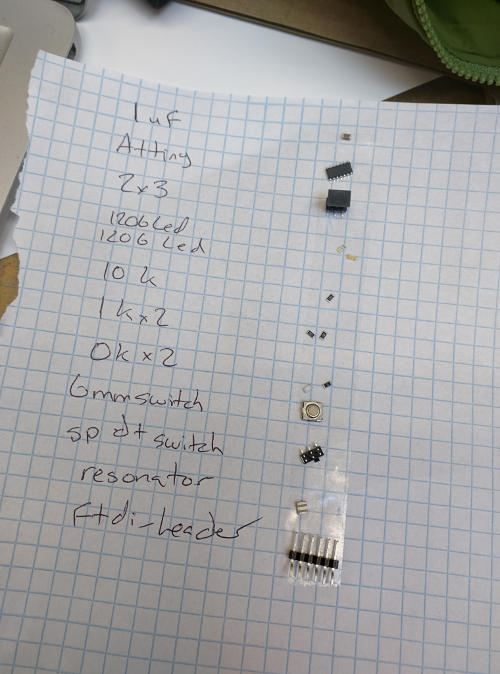
It's nice to collect all of the parts you need on a piece of paper before starting to solder.
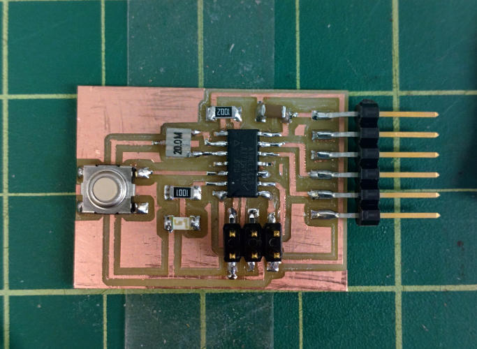
Stuffing the actual circuit boards was pretty straight forward.
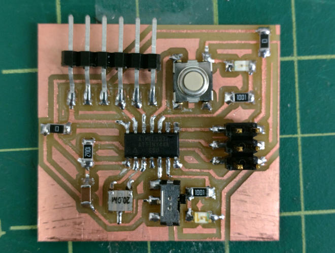
I accidently inverted the outline mask for this board, so as you can see on the far right a trace has been almost removed because the cut was done inside the boundries of the board. You can see the two 0 ohm resistors used as jumpers.
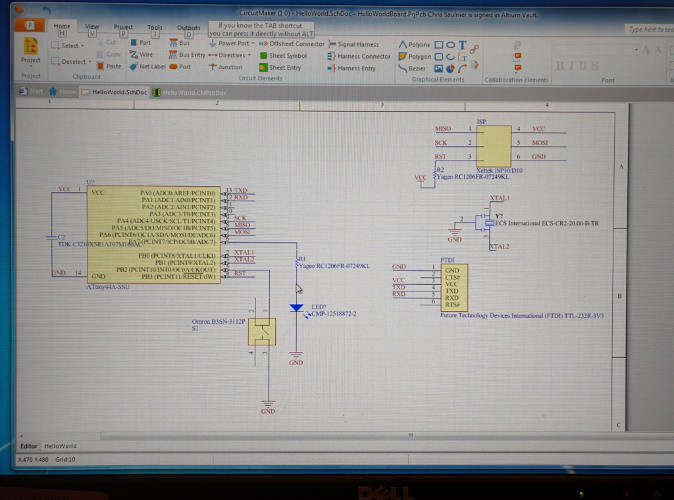
After some success with Eagle I decided to give another of the packages a try. I went with CircuitMaker as it seemed to have some interesting features.
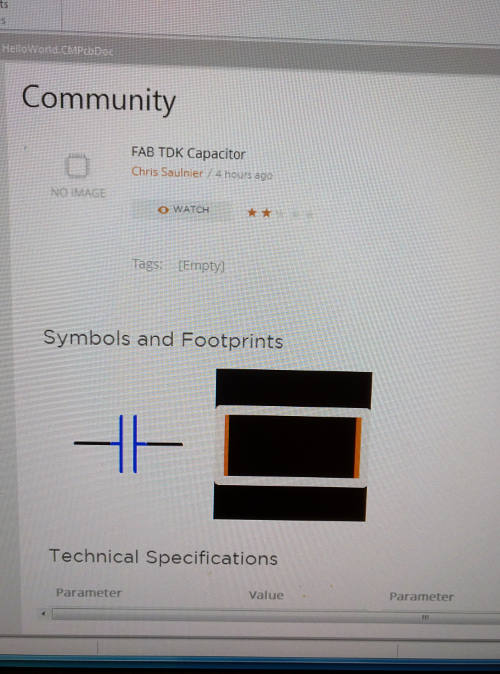
One of which is a shared part library that is user generated. It doesn't have good version control though, as anyone can edit any part at any time and keeping track of revisions (and which revision you are using) is not the most straight forward. I had to make the capacitor we use.
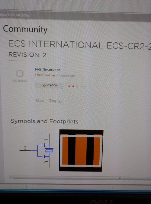
Along with the resonator that we use. The part building interface was pretty straightforward for the most part, and had a handy wizard that helped with some form factors.
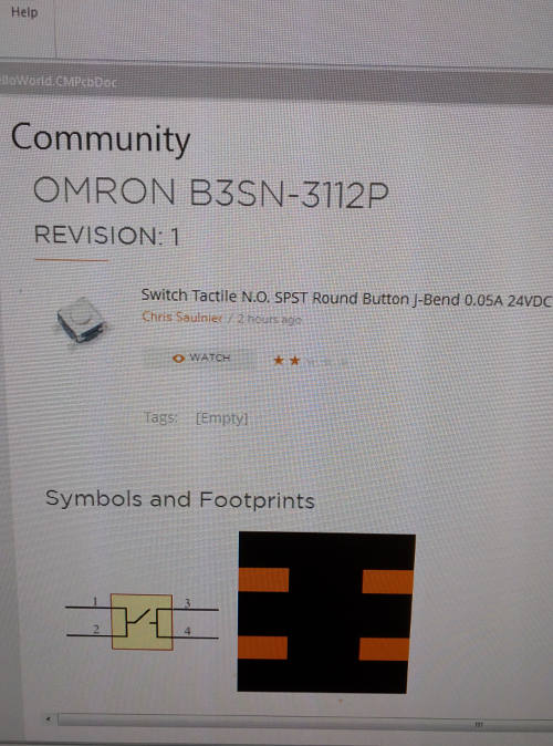
And the switch. Now anyone else should be able to see these parts when they search within CircuitMaker though. No promises that the dimensions are correct, but I did attempt to build the parts based on their datasheets.
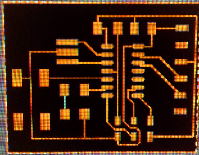
While getting the schematic done up was the slow part, once I started routing CircuitMaker stood out as having some nice features. It does some nice auto-magic as you are placing traces, and does not let you place traces that violate your deign rules. I couldn't figure out an easy way to export the file as an image for milling though.
I wanted to give a design using vias a try. I made my traces 10 mils to solve the previous under-milling issue and then replaced my jumper traces with traces that travelled on the bottom of the board through vias. I figured I would start with trying a fairly large via hole and used the via pads to generate my toolpath at the same time as cutting the outline.
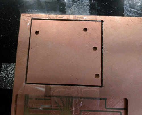
My plan was to mill the top traces, the outline and vias, and then flip it over and tape it in place so that it is in approximately the same place for milling. This worked moderately well, but I didn't get the board to be flat enough so I had a rather deep cut when I milled the back traces, almost going through the whole board. Here you can see the board flipped over before milling the bottom traces.
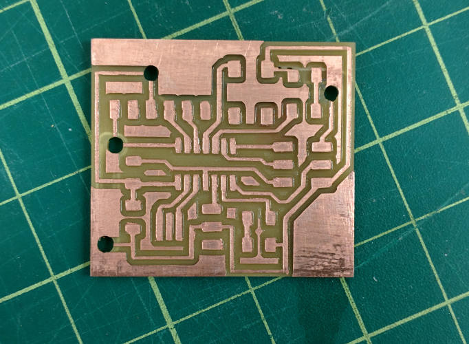
The top view of the traces. In this version of the board I accidently disconnected the respnator from ground in the schematic, luckily I could fix it by using a jumper to connect the resonator to the nearby ground rail.
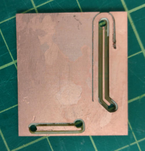
The back came out a little messy. The outer aborted trace is from when I set the outline to 20, I decided to cancel that and use a value of 10 instead. The large vias made for rather difficult connecting between ends. I ended up using 0 ohm resistors as they fit in the holes pretty well. Narrower holes would be more conducive to using thin wires.
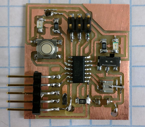
Here is the stuffed V1 board.
I went back and fixed the ungrounded resonator issue, along with making the drill holes for the vias having a diameter of .03937008 (one of the default options...) which was the smallest default, slightly larger than 1/32, that the fabmodules would generate a toolpath for. This should result in a much easier to solder board
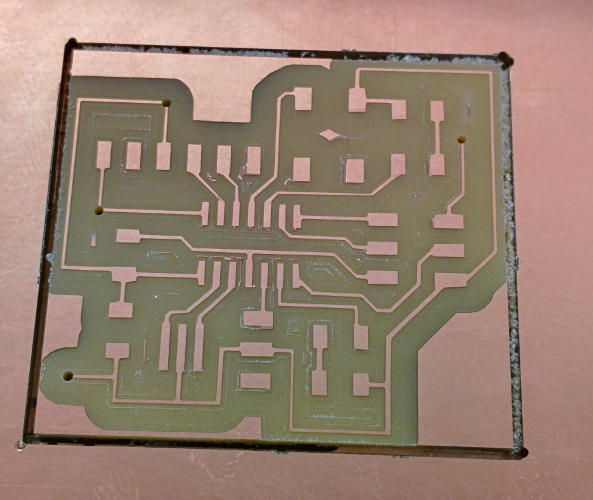
I bumped up the number of outlines so that the vias wouldn't have any copper around them. You can see that the vias are much smaller now. For some reason the vias did not quite go all the way through, but were very very very close, so I could poke out the remaining copper with a wire.
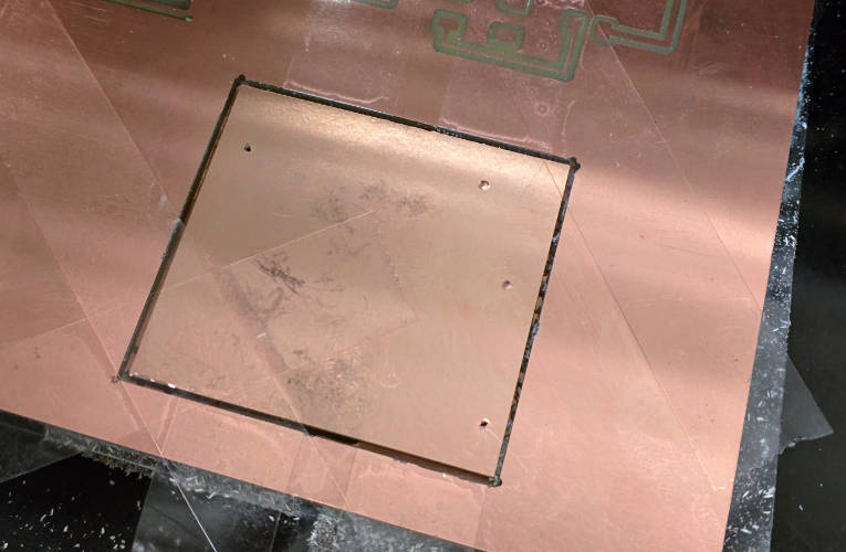
Here you can see the board flipped, taped down, and ready to mill the back traces.

The traces on the back came out well other than a little copper that wasn't quite completely removed. That would be easy to fix with a razor blade. Again I bumped up the number of outlines so that the vias would not be touching any copper but the traces.

The milled board came out really nicely. The smaller vias are much more attractive and 10 mil connectors are a good width.

After some expreimentation I decided the best way to install the vias was to take a 2x3 header, break it down into 1 pin sections and force the connectors through the via hole. The connectors were slightly too big, so once you forced them through they would stay it place due to friction and you could pretty esily get some solder on them and then cut off the extra.

The back of the board with the vias connected.
The finished board with all the vias installed. I got better at it with practice, as you can tell with the via at the top left. Some of the earlier vias were made a bit of a mess by some of my earlier attempts with thinner wire.
For more complex boards I came across the idea of milling two single sided boards and then gluing the boards together. It's difficult to adaquately secure a flipped board down, so that would be a great alternate workflow if you wanted to mill lots of traces on the back of the board.