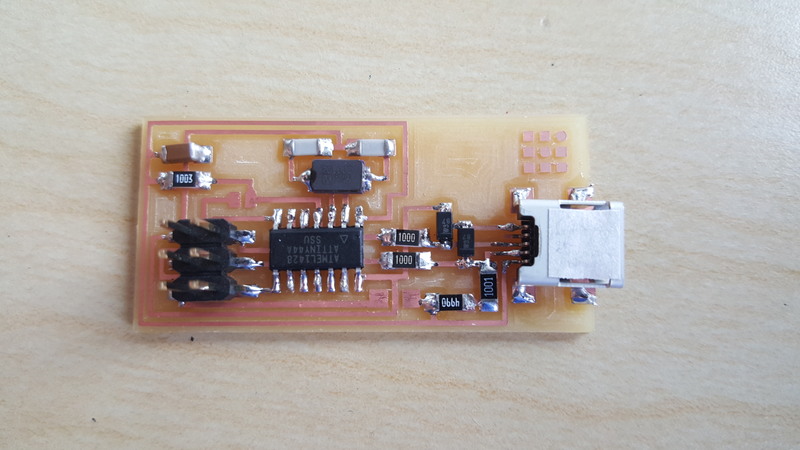
This week's task was to create an In-System Programmer (ISP).
For this intro to e-fab several options for the design files were provided. I chose to use the "Hello ISP" design.
The first and most finely detailed pass carved the edges of the traces with a 1/64" bit. This is the cut that determines how easy or hard it is to solder later, and how much clean up is necessary.
Additional routing passes do not need to the finesse of the first one or two. Gross Routing or Clear Routing was done with a 1/32" bit to speed up this process.
Note that the Tool diameter is intentionally set incorrectly as larger than the actual diameter. This ensures that it does not touch the trace edges that the 1/64" bit established, and effectively reduces the Offset Overlap. Nominal Offset Overlap was kept at 50%, but with experimentation may be able to be reduced. Again, this operation does not need to leave beautiful edges, it is a clear cut.
This step was run with the default settings. The correct bit is already loaded and zeroed from the previous step, so it can be run immediately after the Gross Routing finishes.
Board stuffing was done by hand with a standard soldering iron, leaded solder, a pair of non-esd safe tweasers, and a dental pick. A few component specific notes:
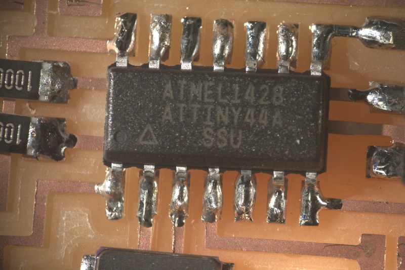
This was the easiest component to stuff, and is a good candidate for a start component. Orient the part so that pin 1 (dot) is closest to the USB connector. Tack solder pin 1, and check orientation on the opposite pin (pin 8). If its placement needs adjustment, repeatedly tap pin 1 with the iron so the solder is wet but not overly hot. The viscosity of the solder should be sufficiently high to resist motion of the part. Use the dental pick to push the component around until alignment is good. Push down gently so that all pins are flush to their pads.
With the first pin attached, solder the other 3 pins. Solder in an "X" - pin 1, 8, 14, 7.
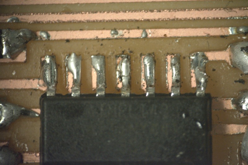
This figure shows the result of heating only the pin and not the pad. This is characterized by the solder balling up away from the pad, with the surface tension fighting the bond. For example, the middle pad shows the right amount of solder, but it has not flowed on the pad. The speckled pad surface shows where solder froze immediately on contact with the cold pad, and the horizontal knit line shows two separate thermal events - the final time the solder was melted, only part of it wet. The rest remained in its previous configuration
When this happens, apply heat directly to both pad and pin.
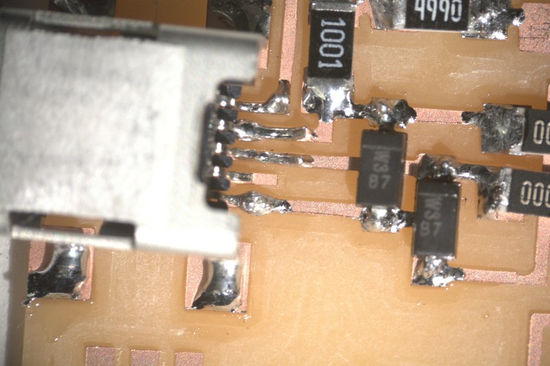
This was the most difficult component to stuff due to its narrow trace pitch and the occlusion from the connector hood. This 5-step process worked well:
Place the connector on the circuit board and visually align it. Use the narrow connector pins for horizontal alignment, and the wide shell mounting pads for vertical alignment. The tweasers give a false sense of accuracy - the connector will jump when they let go. Pushing with the dental pick seems harder, but is worth while.
Tack a far corner down with a medium amount of solder. For this pin the ability to re-wet it and move it is more important than cleanliness, so don't be overly conservative. The increased thermal mass and the increased iron target size later.
It is nearly guaranteed that the connector moved during this process. Heating the single solder joint should give about a second of wetness before it re-freezes. Use the back end of the tweasers or the dental pick to gently tap it into orientation. Once its angle and x y are correct, push down on the center of the connector and re-wet the solder briefly. This should bring it flush to the board.
Use the binocular microscope to verify orientation and alignment. It may be helpful to bring the focal point an inch or two above the work surface of the scope. This will allow you to rotate the board to look at the pins better.
If the placement is incorrect, gently fix it as described above.
Solder the remaining 3 ground tabs. Use less solder on these joints than on the first one. Press the iron tip to the top of each tab, and tap the solder to the side where the tab meets the pad. The solder should wick around the corner.
The key to these pins is to use as little solder as possible and to take advantage of solder's surface tension. Apply a very small amount of solder to the iron's tip. If there is too much, clean it off and repeat. Tap the iron down on the trace just outside the connector body and hold it there. Slowly move towards the pin until the solder "jumps" towards the pin. When this occurs, stop moving the iron and wait for 2-4 seconds before lifting the tip.
DO NOT TOUCH THE IRON TO THE CONNECTOR DURING THIS PROCESS
The solder jumps when the pin is sufficiently warm and the solder is sufficiently near. Heating the adjacent pins will make it easy for the solder to bridge to them. It is much easier to selectively heat using the traces as thermal conductors - the traces are flat and easy to push down on.
Note: The "ID" pin is not necessary for this application and can be left alone.
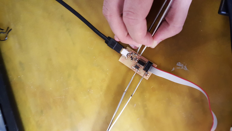
Plug in the programming and USB cables. This unfortunately torques the board, which can make it difficult to fix orientation of the board. An extra pair of hands is helpful for this process, but not necessary. Fix the board to the table by pushing down on it or taping it. Place two pairs of non-ESD safe metal hook-tipped tweasers in the locations shown.
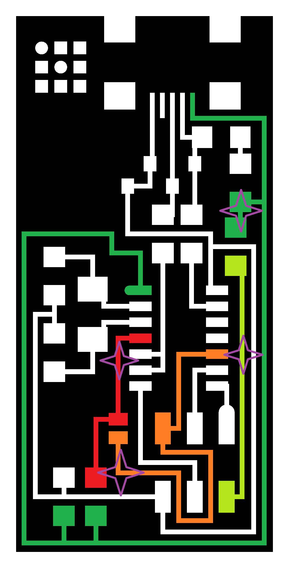
One tweaser shorts between the red and orange nets. The other shorts between the green and yellow nets. Suggested contact points marked in purple. The tweaser should be relaxed during programming.