This week I focused on manufacturing circuit boards using the Trotec Speedy 100 Flexx
This 2-in-1 laser cutter features both a CO2 laser and a fiber laser. The CO2 laser can cut the FR1 substrate, but cannot cut copper - the beam simply reflects, unabsorbed. The fiber laser can cut copper because it is a different wavelength, but has difficulty with the FR1 substrate.
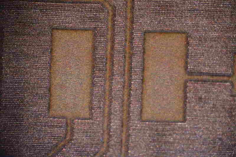
Two traces between pads in the ISP header
The Trotec laser can achieve much smaller feature sizes than the Roland mill can. The native resolution is 1 mil (1 thousandth of an inch), but the smallest I could reliably create was 7 mil trace and space.

Trace and Space Testing
Very small traces (<3 mil) are completely destroyed. Traces up to 5 or 6 mil may look usable, but these often delaminated and/or were prone to breaking. Above 7 mil the traces were great, though without etching correction they end up slightly smaller than designed.
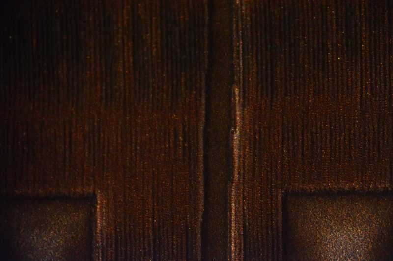
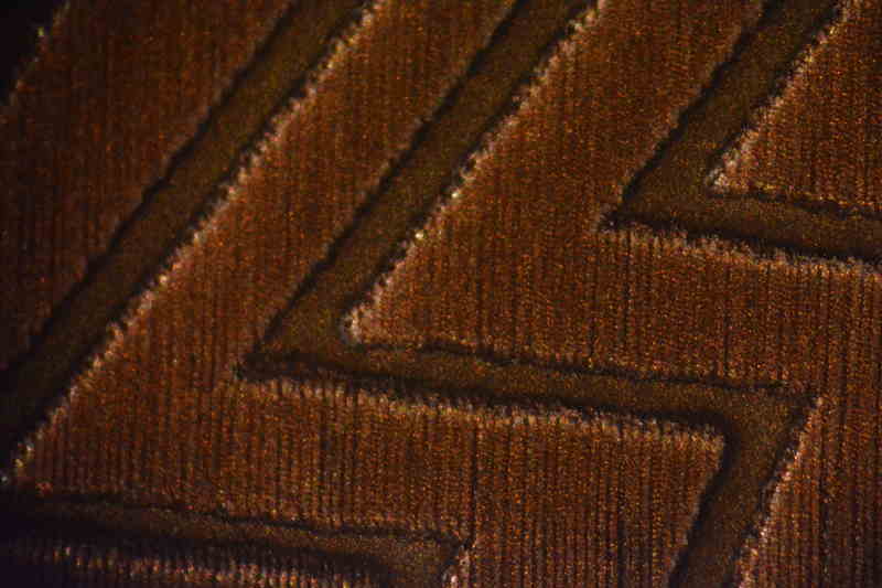
The laser is rastering to cut the traces, so there is pixelation in the resulting product. This shows up readily in traces routed on a diagonal, as shown above.
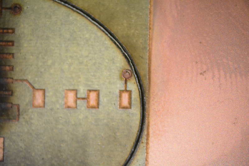
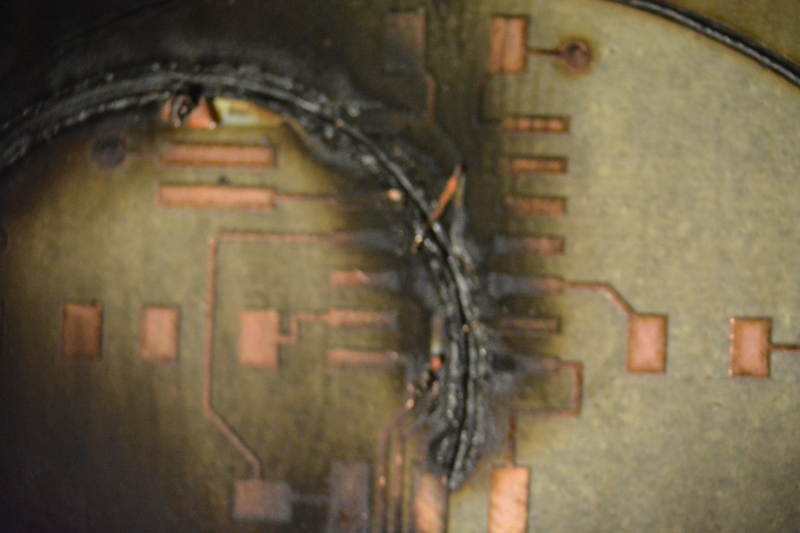
PCB outline and Via