This week was an experiment in how small a part I could work with. This was a painful experiment.
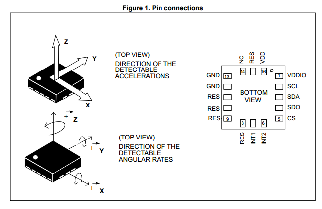
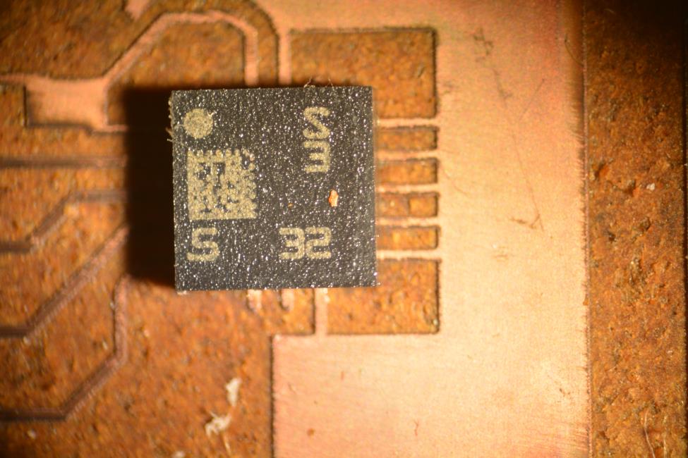
The LSM6DS33 (http://www.st.com/web/en/resource/technical/document/datasheet/DM00157718.pdf) is a 6 axis Inertial measurement unit from ST. It contains a 3 axis accelerometer and a 3 axis rate gyroscope, all within a 3mm x 3mm x 0.86mm 16 pin Land Grid Array package.
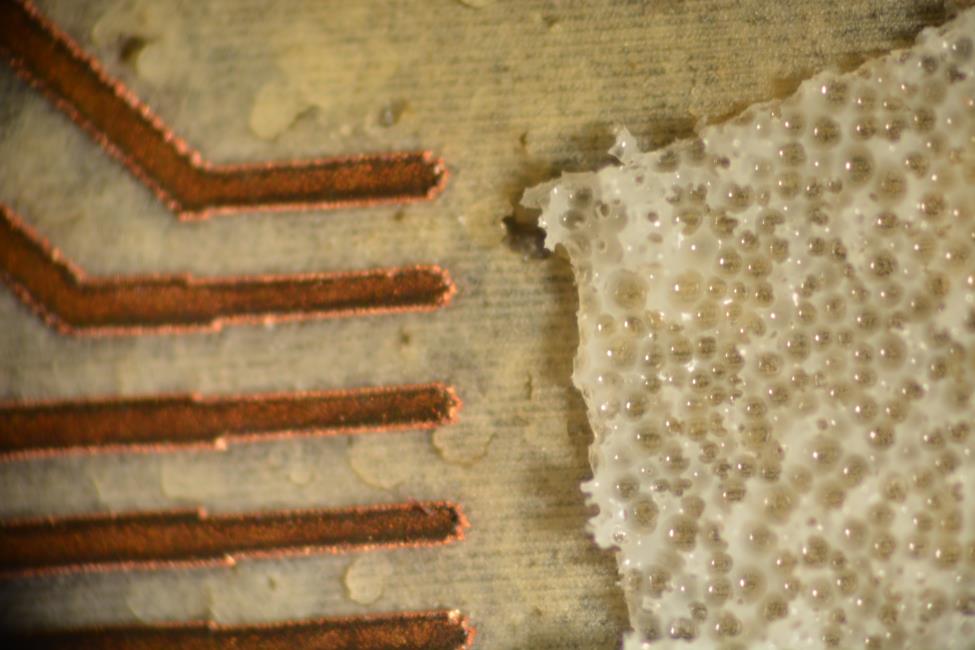
LGA packages are notoriously difficult to solder. The pads are recessed by 0.1mm and therefore not visible when the part is on the circuit board, which means that traditional use of a soldering iron is not possible. The pads are on a 0.5mm pitch, and 0.25mm wide.
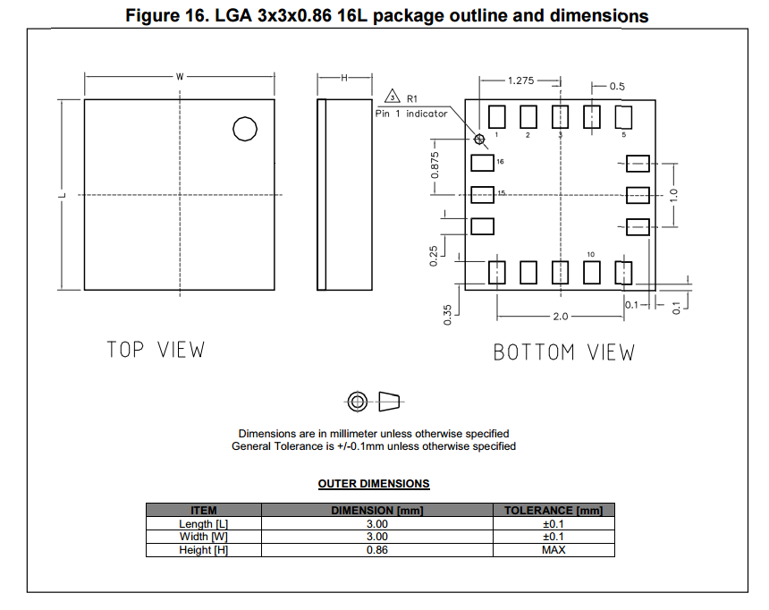
These packages are typically stuffed by using a combination of solder paste, solder mask, and a reflow oven. The guidelines for this package ask for the solder stencil to be aligned to within 25 microns. Fancy.
The 0.5mm pitch is equivalent to just under 20 mil, so I needed a kerf on the order of half of that. I tried the .010" endmill on the modella and the trotec fiber laser. Both have resolutions on the order of 1 mil, so I'm only limited on spacing between pads - the pads themselves can be smaller as necessary.
I tried using the CO2 laser for silk screening. This left ugly burn marks
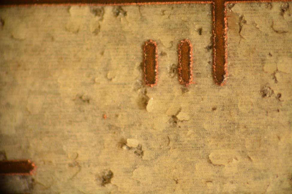
With the right settings dialed in, the Laser produced beautiful pads. These are the smallest I was able to reliably recreate.
This run wasn't sufficiently taped
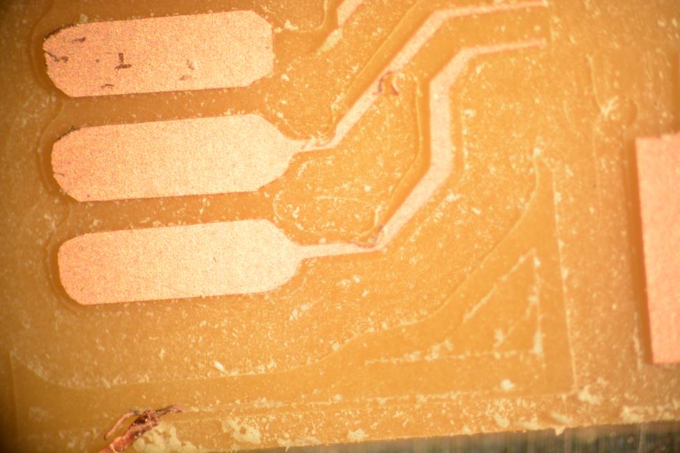
This is usually my go to for geometries like this, but I ran into a couple issues.
Dispensing the paste was unusually difficult. I usually control the amount of solder applied to a pad with a regulated compressed air source - each tap on the foot pedal releases a known amount of air, which pushes a known amount of solder out. I was doing this part manually instead, and there was an unexpected amount of compliance in the applicator. This meant that the paste would continue to dispense 30 seconds after tapping the plunger!
More worrying, the beads didn't actually flow during reflow. Adjacent tests in the same batch flowed fine, so I'm wondering if I was accidentally using RoHS compliant paste instead of actual solder paste. If I were to retry this method, I'd bump the max temperature up.
Insufficient temperature during reflow?
TL;DR; Don't use unlabeled paste of unknown provenance.
I used to use this method for iron-soldering small passive components, but it can be difficult to level the part. I thought I'd try it on this package.
Use an iron to put solder on each of the pads. Manually align the part, reflow in the oven.
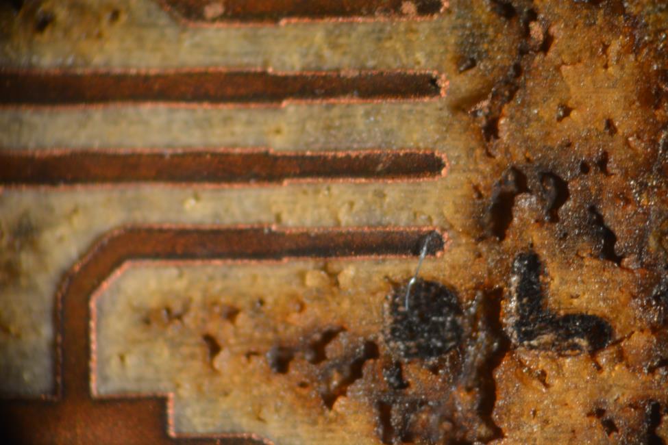
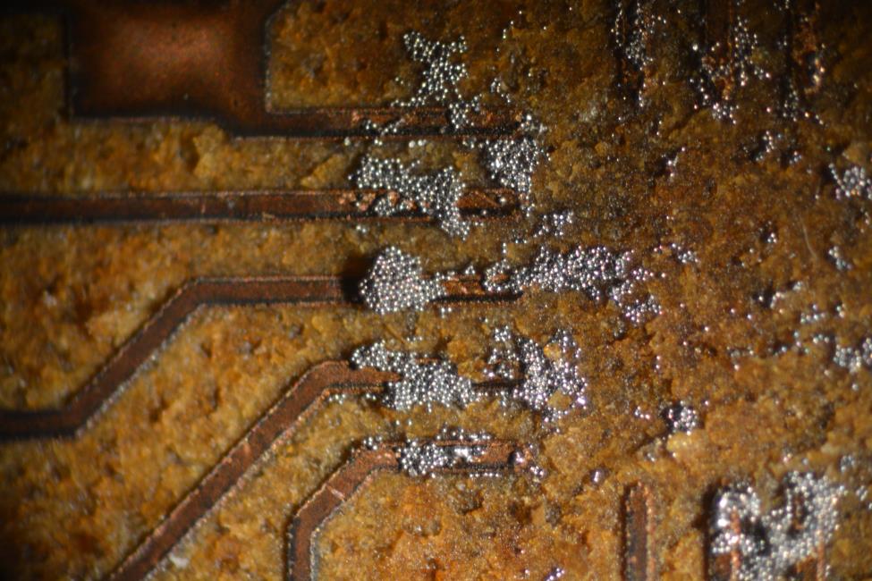
I had difficulty controlling where the solder went. It wicked away from the pad along the trace to the giant ground-pour. Typically I "neck" the pad - make sure the trace coming away from the pad is significantly more narrow than the pad itself. This helps control heat flow during manual soldering. I was already at the smallest feature size I could hit with this process, so that was not an option. Additionally, the lack of soldermask meant I had nothing to block the wicking.
Severe Wicking
After reflow one firm tap of the board and the part fell off.
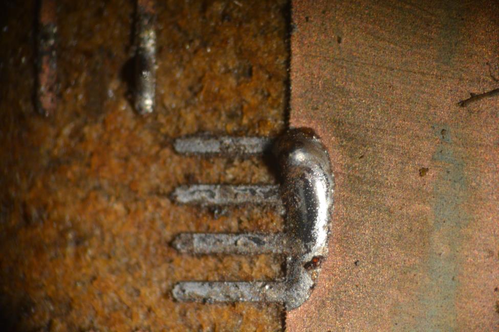
Solder bumping is essentially pre-tinning the pads of the package, which ends up looking a lot like making a BGA out of your LGA.
This worked pretty well! I think with a little practice this could be reasonably reliable. XRay Imaging
Since the pads of an LGA aren't visible, you can't see how well they ponded with visible light. I put one of the boards in the Micro CT scanner. You can see that this one didn't flow much - the dark black spots are the solder, which hasn't spread since its initial bumping.
You can also see die-bonding wires inside the package, even smaller than the ones I used.
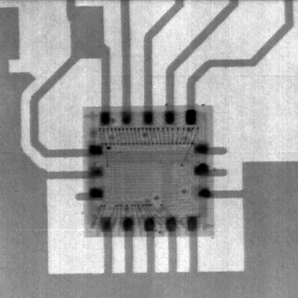
Front View
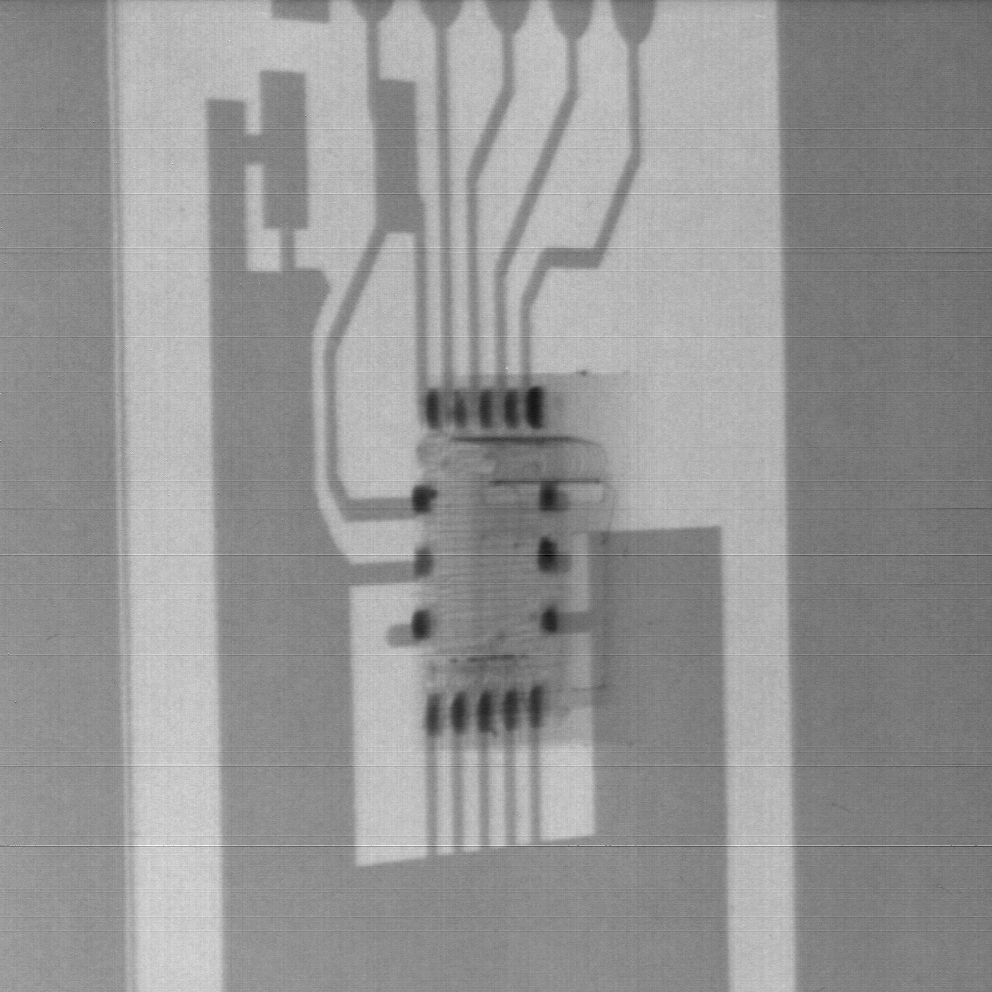
Side View
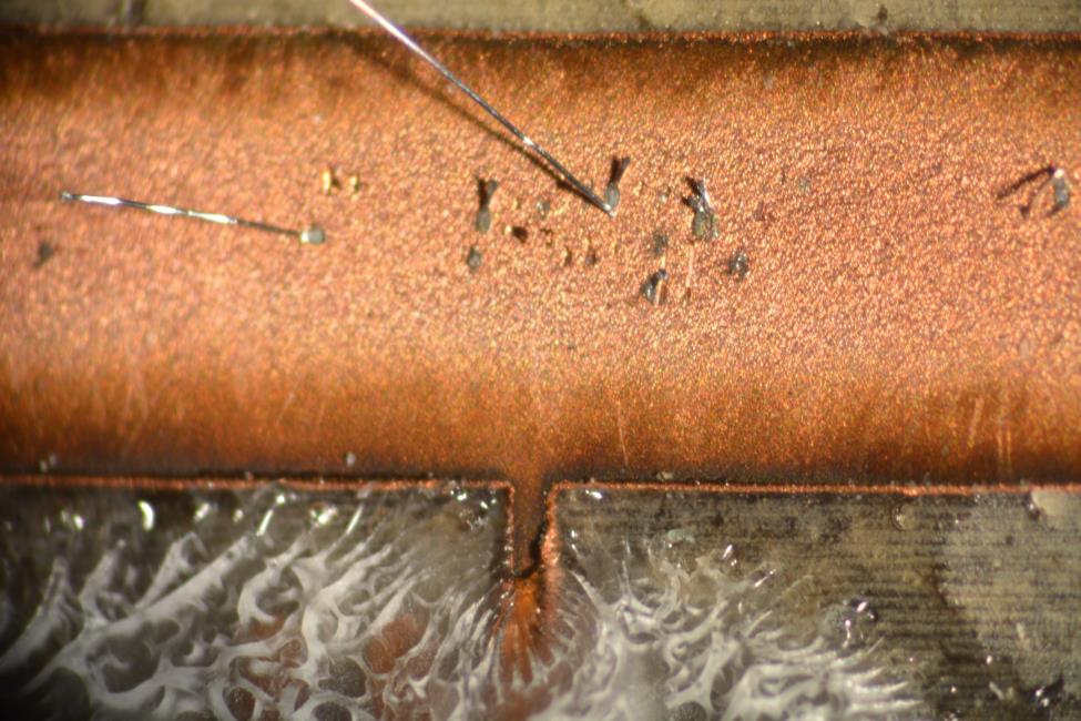
This method was a lot of fun, though admittedly frustrating. Rather than using solder, this method welds very tiny wires between the part and the circuit board.
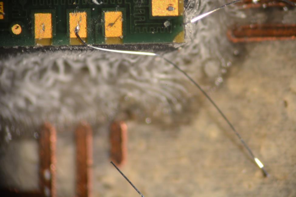
The machine can be comparatively finicky, but it can be very effective once it is dialed in (until the tip clogs). Of the techniques I tried, this is the only one that lets you actually see the connections you are making as you are making them. This allows you to detect and adjust for errors, rather than wait to the end and hope. Also, the pads on the board don't have to line up with the pads on the chip. You can use a wider spacing on the board, which makes it easier to mill.
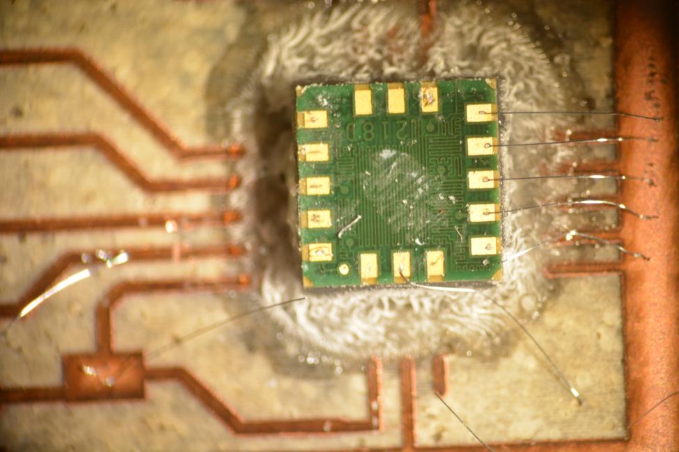
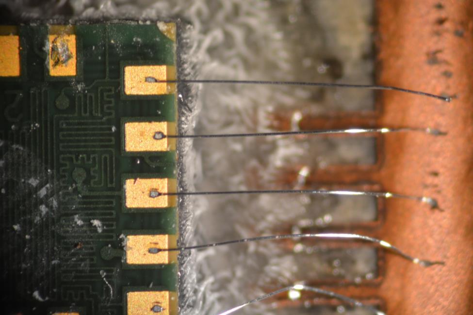
5 successful bonds in a row, all to ground.
VHB was too squishy
Practice on some big pads before going for the actual part
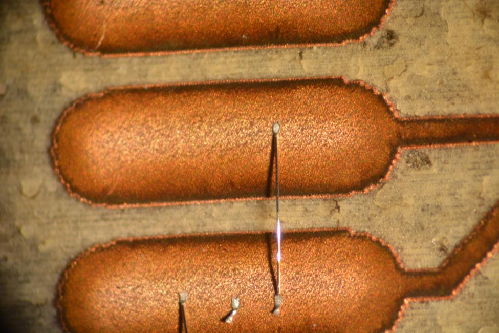
Mill the board. Even minor scorching from the laser makes it difficult to weld the starting wire.
The tip is very directional, and will only weld the second bond if the wire is coming out straight down.
This bond broke off because the attack angle was wrong. Pry it off with tweasers.
You'll need a big empty piece of copper nearby to clean off the tip. A ground pour works well for this. Alternatively, don't cut out the board outline.