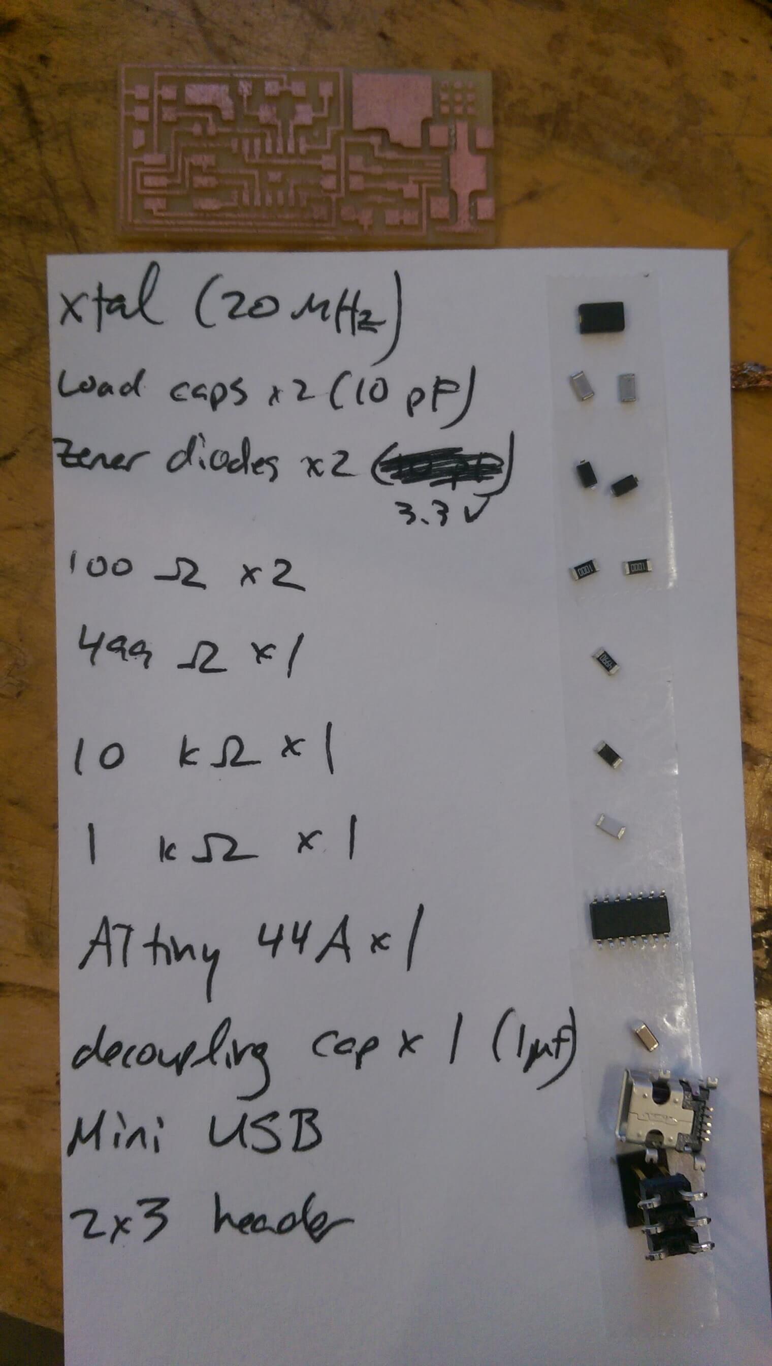
week 2: milling and stuffing an ISP PCB
For this week, I milled a printed circuit board (PCB) in-system programmer (ISP) that can be used as a USB peripheral to program other circuit boards and embedded devices.
milling attempt number 1 (a failure)
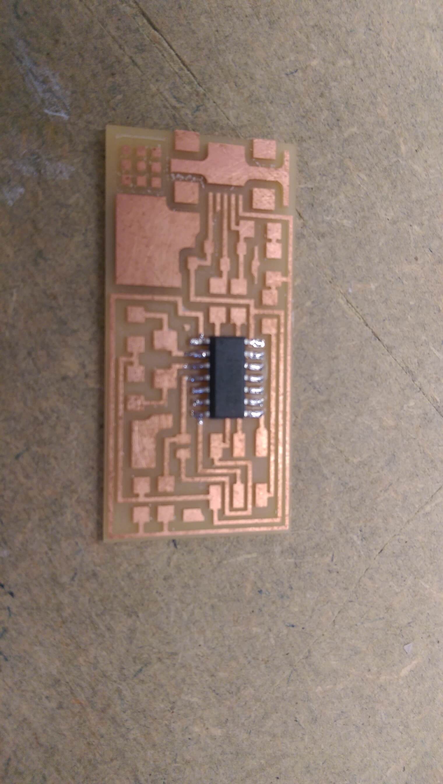
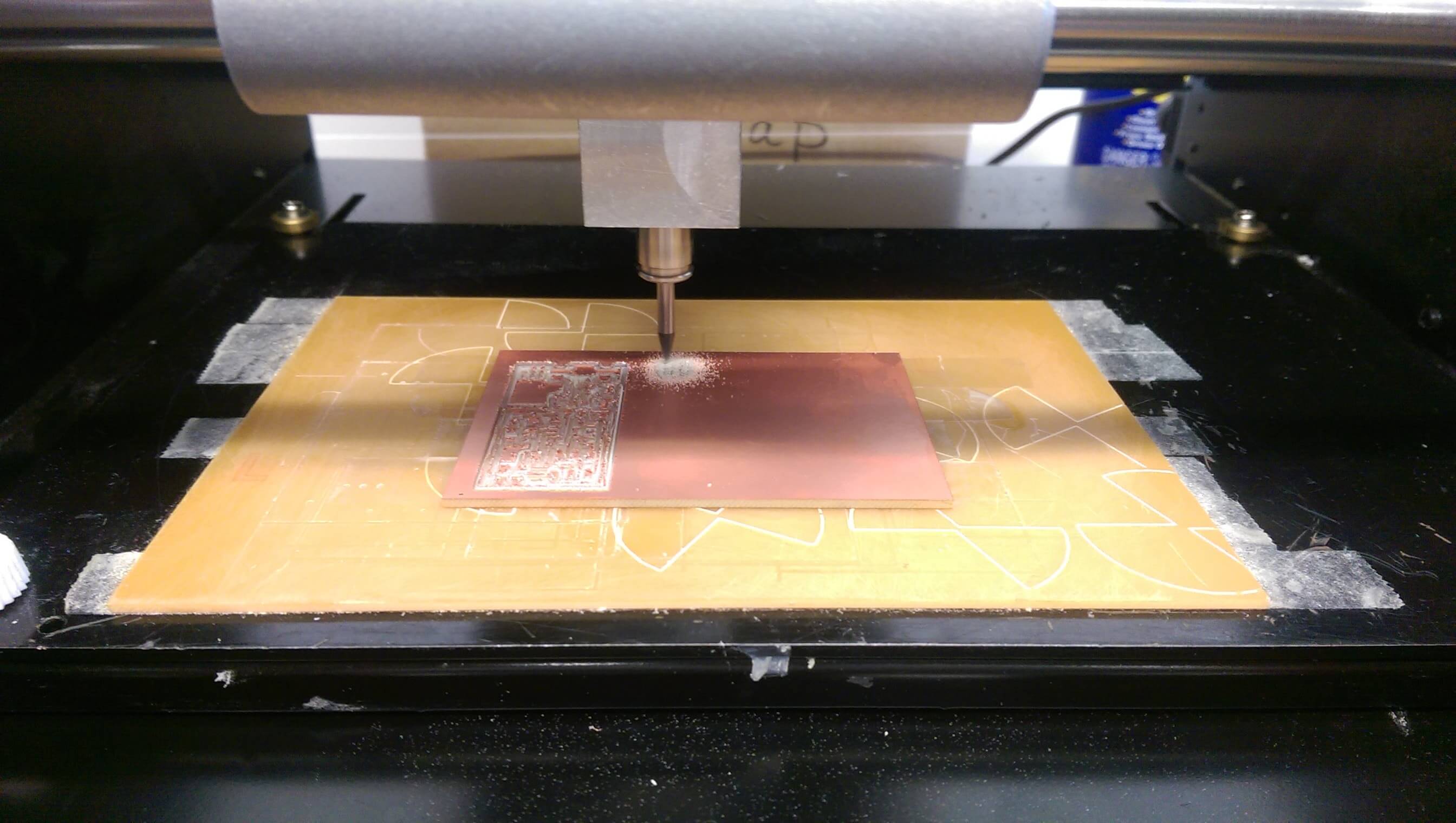
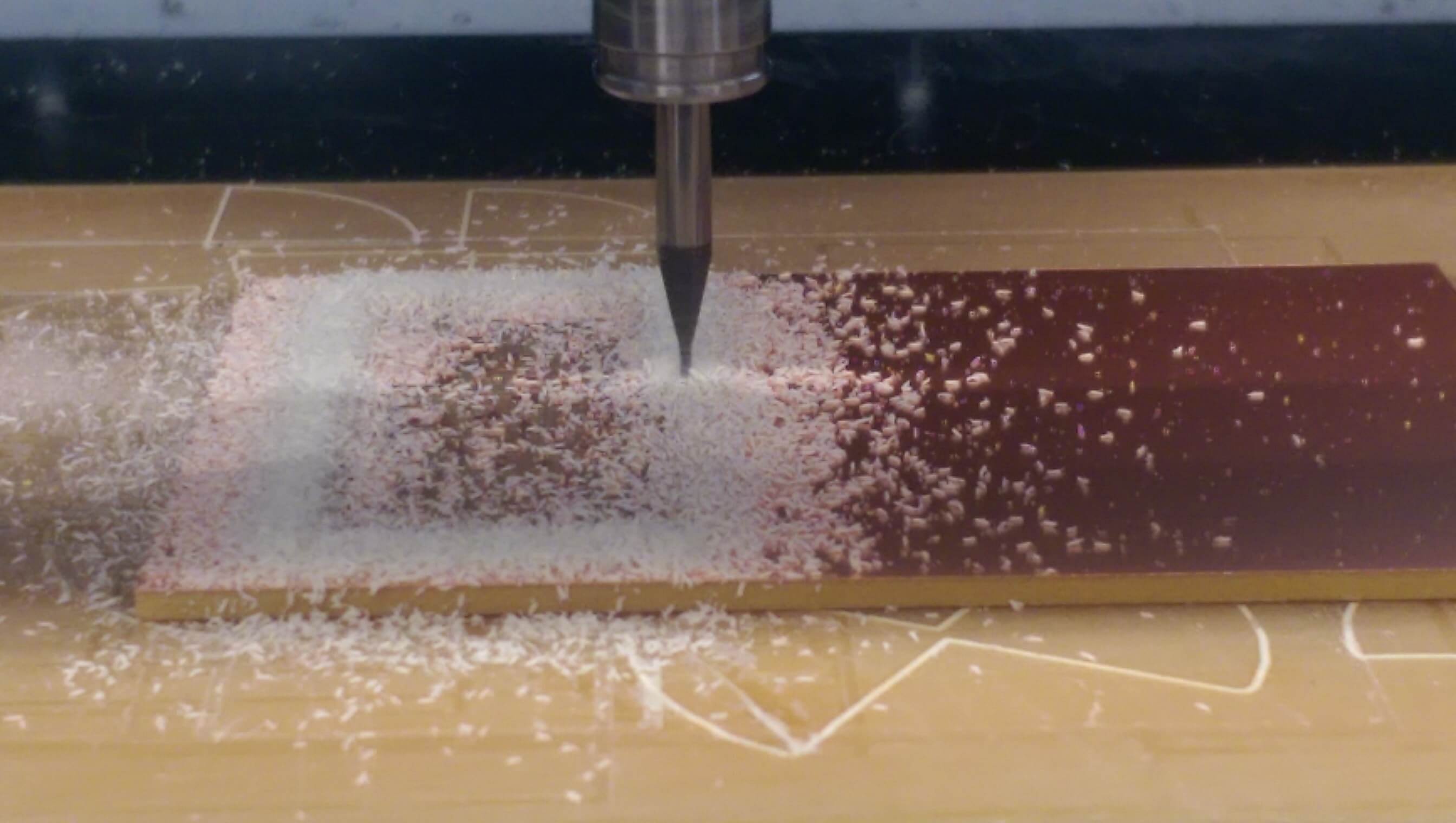
To fabricate the PCBs, we use a desktop Roland milling machine controlled via the fab modules. To avoid milling glass (and thus creating asbestos-like silica particles) we use custom copper plate stock with a plastic layer underneath. I first cut the board traces with a 1/64" end mill, and then released the board from the sacrificial plastic layer with a 1/32" outline.
My first milling attempts (see above) were rather unsuccessful: on the first attempt, the board was not milled at all; to compensate, I pressed the end mill down *rather* hard while fastening the screws to zero the mill. The result was a cut that was much too deep, and that abolished the topology of the circuit. Inspecting the end mill under a microscope revealed that it had lost its edge; replacing the endmill and more judiciously zeroing the system resulted in a clean, elegant cut. I learned that part of the zen of milling PCBs requires recognizing "the right amount of dust": enough to mostly cover your pattern, but a light enough dusting that you can still make out your features *as the mill is cutting*.
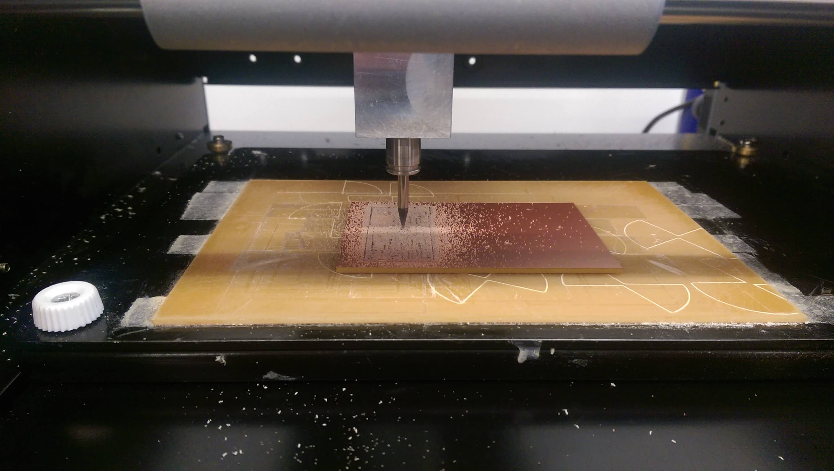
succesful PCB milling: the right amount of dust
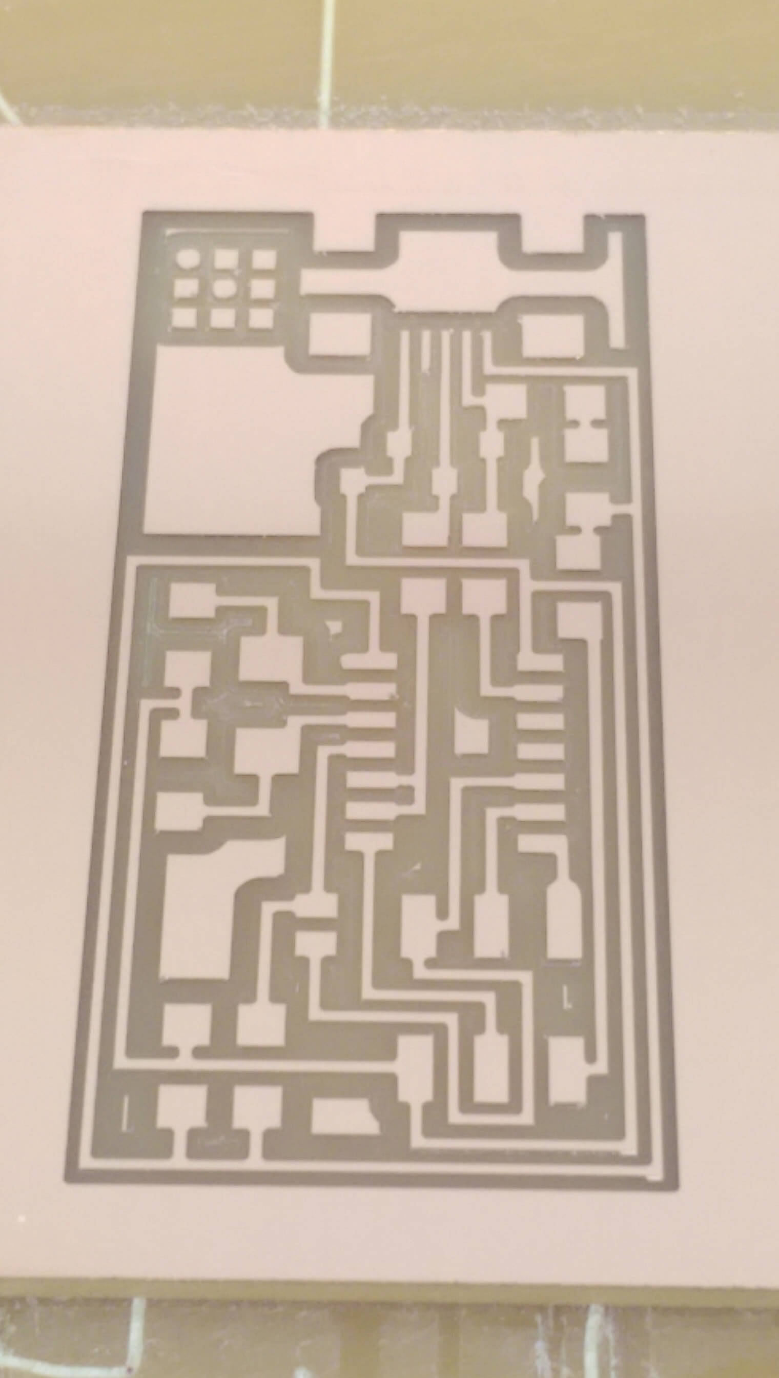
completed board
liberated board after outline trace
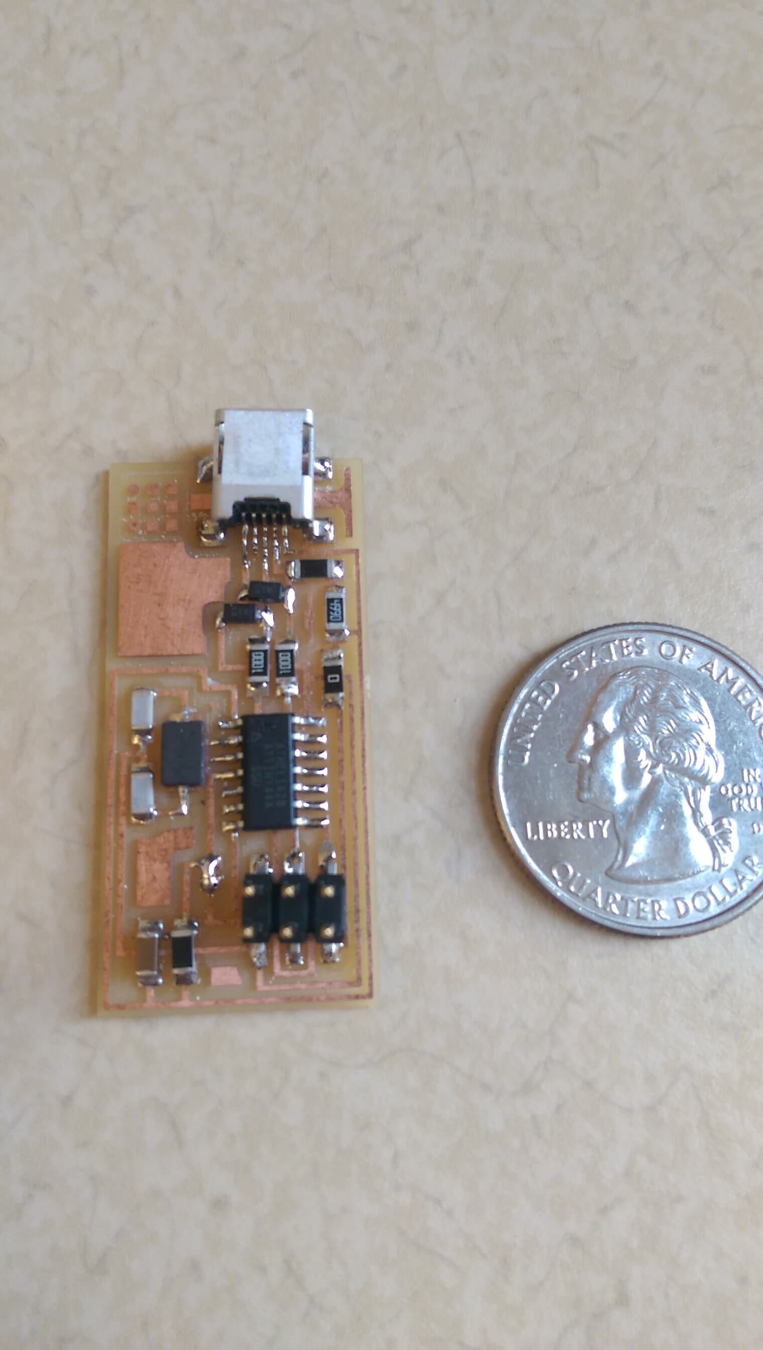
Due to a peculiarity of our section's workflow, my final board ended up not being this one, but rather another board that had been cut earlier (we exchanged soldering and milling shifts, and I happened to solder before I milled). Working inside-out and from small to large components, I elected to solder the ATtiny44 microchip first since its geometry was somewhat more delicate. I then worked outwards, finishing with the USB port. I soldered one jumper with a large solder blob, and another with a 0 Ohm reister (to bridge another trace).
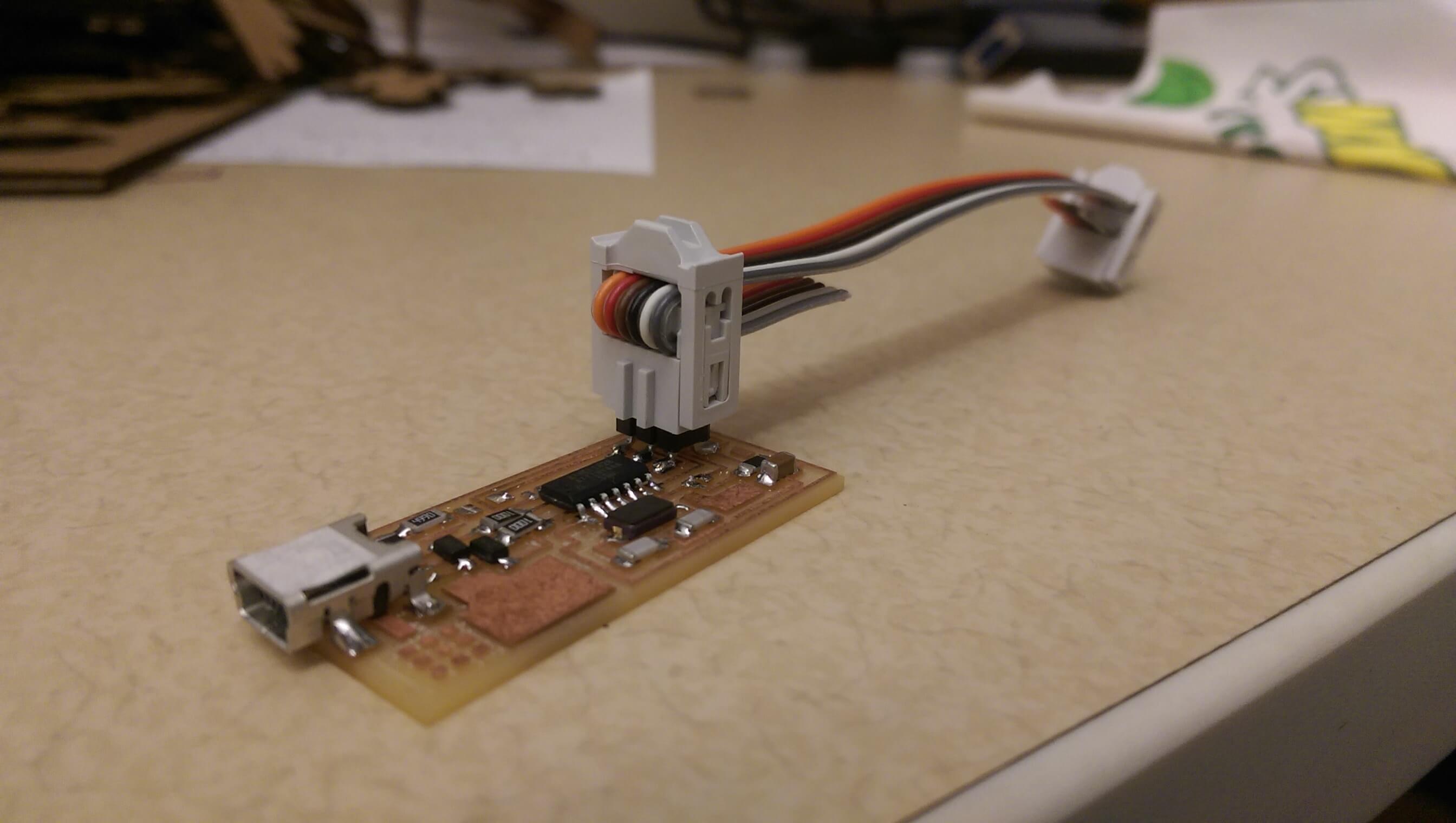
After my initial soldering pass, my chip did not draw enough voltage from the USB port (i.e. I measured ~ 1.35 V rel. to ground rather than 5 V on the microchip). Liberally resoldering the USB connections (and then wicking away the excess) resolved the problem, and the ISP programmed successfully. I then removed the jumpers and, to my despair, my laptop didn't recognize the FabISP when connected to a USB port. Poking around with a voltmeter revealed that one resistor in the upper part of the board was poorly connected - liberally resoldering that connection fixed the issue and allowed my laptop to recognize the device.