XML Structure of an Eagle Library File
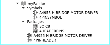
For this tutorial, I am using a Library file called myFab.lbr that contains 2 symbols, 2 packages, and 2 devices as shown in the image below. If you don't know the relationship between symbols, packages, and devices in Eagle, you can check out Creating Components in Eagle (Almost) Frustration-Free. Basically, a device consists of a symbol and a package. The symbol is the schematic representation and the package is the actual geometric profile of the device.
An Eagle library is a file that ends with the .lbr extension and it contains XML content that describes all the devices, packages, and symbols contained in the library. You can view and edit an .lbr file with any text editor, but I would recommend SublimeText. If you open an .lbr file, you will find it not very easy to read because it is not indented propery. But that can easily be fixed by cutting and pasting the contents into http://www.cleancss.com/xml-beautify/ and then copying the output back into the .lbr file. After this step the XML becomes relatively easy to read and understand. Here is the XML content of myFab.lbr (To display the XML on this page I used the tool http://www.freeformatter.com/html-escape.html.):
<?xml version="1.0" encoding="utf-8" ?>
<!DOCTYPE eagle SYSTEM "eagle.dtd">
<eagle version="7.4.0">
<drawing>
<settings>
<setting alwaysvectorfont="no" />
<setting verticaltext="up" />
</settings>
<grid distance="0.1" unitdist="inch" unit="inch" style="lines" multiple="1" display="no" altdistance="0.01" altunitdist="inch" altunit="inch" />
<layers>
<layer number="1" name="Top" color="4" fill="1" visible="yes" active="yes" />
<layer number="16" name="Bottom" color="1" fill="1" visible="yes" active="yes" />
<layer number="17" name="Pads" color="2" fill="1" visible="yes" active="yes" />
<layer number="18" name="Vias" color="2" fill="1" visible="yes" active="yes" />
<layer number="19" name="Unrouted" color="6" fill="1" visible="yes" active="yes" />
<layer number="20" name="Dimension" color="15" fill="1" visible="yes" active="yes" />
<layer number="21" name="tPlace" color="7" fill="1" visible="yes" active="yes" />
<layer number="22" name="bPlace" color="7" fill="1" visible="yes" active="yes" />
<layer number="23" name="tOrigins" color="15" fill="1" visible="yes" active="yes" />
<layer number="24" name="bOrigins" color="15" fill="1" visible="yes" active="yes" />
<layer number="25" name="tNames" color="7" fill="1" visible="yes" active="yes" />
<layer number="26" name="bNames" color="7" fill="1" visible="yes" active="yes" />
<layer number="27" name="tValues" color="7" fill="1" visible="yes" active="yes" />
<layer number="28" name="bValues" color="7" fill="1" visible="yes" active="yes" />
<layer number="29" name="tStop" color="7" fill="3" visible="no" active="yes" />
<layer number="31" name="tCream" color="7" fill="4" visible="no" active="yes" />
<layer number="53" name="tGND_GNDA" color="7" fill="9" visible="no" active="no" />
<layer number="54" name="bGND_GNDA" color="1" fill="9" visible="no" active="no" />
<layer number="90" name="Modules" color="5" fill="1" visible="yes" active="yes" />
<layer number="91" name="Nets" color="2" fill="1" visible="yes" active="yes" />
<layer number="92" name="Busses" color="1" fill="1" visible="yes" active="yes" />
<layer number="93" name="Pins" color="2" fill="1" visible="yes" active="yes" />
<layer number="94" name="Symbols" color="4" fill="1" visible="yes" active="yes" />
<layer number="95" name="Names" color="7" fill="1" visible="yes" active="yes" />
<layer number="96" name="Values" color="7" fill="1" visible="yes" active="yes" />
<layer number="97" name="Info" color="7" fill="1" visible="yes" active="yes" />
<layer number="98" name="Guide" color="6" fill="1" visible="yes" active="yes" />
<layer number="100" name="Muster" color="7" fill="1" visible="no" active="no" />
<layer number="101" name="TEXT" color="7" fill="1" visible="yes" active="yes" />
<layer number="250" name="Descript" color="3" fill="1" visible="no" active="no" />
<layer number="251" name="SMDround" color="12" fill="11" visible="no" active="no" />
</layers>
<library>
<packages>
<package name="4HEADERPINS">
<smd name="1" x="0" y="1.27" dx="2.54" dy="1.27" layer="1" />
<smd name="2" x="0" y="-1.27" dx="2.54" dy="1.27" layer="1" />
<smd name="3" x="0" y="-3.81" dx="2.54" dy="1.27" layer="1" />
<smd name="4" x="0" y="-6.35" dx="2.54" dy="1.27" layer="1" />
<text x="-1.905" y="-5.715" size="1.27" layer="25" rot="R90">>NAME</text>
<text x="-0.889" y="1.016" size="0.6096" layer="21">VCC</text>
<text x="-0.889" y="-1.524" size="0.6096" layer="21">GND</text>
<text x="-0.889" y="-6.731" size="0.6096" layer="21">Out2</text>
<text x="-0.762" y="-4.064" size="0.6096" layer="21">Out1</text>
</package>
<package name="SOIC8">
<description><B>Wide Plastic Gull Wing Small Outline Package</B></description>
<wire x1="0.98" y1="3.87" x2="1.23" y2="3.62" width="0.1524" layer="21" curve="-90" cap="flat" />
<wire x1="1.23" y1="-1.08" x2="0.98" y2="-1.33" width="0.1524" layer="21" curve="-90" />
<wire x1="-3.77" y1="-1.08" x2="-3.52" y2="-1.33" width="0.1524" layer="21" curve="90" cap="flat" />
<wire x1="-3.52" y1="3.87" x2="-3.77" y2="3.62" width="0.1524" layer="21" curve="90" cap="flat" />
<wire x1="1.23" y1="-1.092" x2="1.23" y2="3.61" width="0.1524" layer="21" />
<wire x1="-3.77" y1="-1.092" x2="-3.77" y2="3.61" width="0.1524" layer="21" />
<wire x1="0.98" y1="3.87" x2="-3.51" y2="3.87" width="0.1524" layer="21" />
<wire x1="-3.52" y1="-1.33" x2="0.98" y2="-1.33" width="0.1524" layer="21" />
<circle x="-2.385" y="2.69" radius="0.5" width="0.0508" layer="21" />
<smd name="1" x="-4.424" y="3.175" dx="0.5" dy="2.2" layer="1" rot="R270" />
<smd name="2" x="-4.424" y="1.915" dx="0.5" dy="2.2" layer="1" rot="R270" />
<smd name="3" x="-4.424" y="0.645" dx="0.5" dy="2.2" layer="1" rot="R270" />
<smd name="4" x="-4.424" y="-0.625" dx="0.5" dy="2.2" layer="1" rot="R270" />
<smd name="8" x="1.884" y="3.175" dx="0.5" dy="2.2" layer="1" rot="R270" />
<smd name="7" x="1.884" y="1.905" dx="0.5" dy="2.2" layer="1" rot="R270" />
<smd name="6" x="1.884" y="0.635" dx="0.5" dy="2.2" layer="1" rot="R270" />
<smd name="5" x="1.884" y="-0.635" dx="0.5" dy="2.2" layer="1" rot="R270" />
<text x="-3.429" y="4.1275" size="1.27" layer="25" ratio="10">>NAME</text>
<text x="-3.429" y="-2.794" size="1.27" layer="27" ratio="10">>VALUE</text>
</package>
</packages>
<symbols>
<symbol name="4PINSYMBOL">
<pin name="1" x="2.54" y="7.62" length="short" />
<pin name="2" x="2.54" y="5.08" length="short" />
<pin name="3" x="2.54" y="2.54" length="short" />
<wire x1="12.7" y1="9.398" x2="5.08" y2="9.398" width="0.254" layer="94" />
<wire x1="5.08" y1="9.398" x2="5.08" y2="-1.524" width="0.254" layer="94" />
<wire x1="5.08" y1="-1.524" x2="12.7" y2="-1.524" width="0.254" layer="94" />
<wire x1="12.7" y1="-1.524" x2="12.7" y2="9.398" width="0.254" layer="94" />
<pin name="4" x="2.54" y="0" length="short" />
</symbol>
<symbol name="A4953-H-BRIDGE-MOTOR-DRIVER">
<wire x1="-20.32" y1="13.97" x2="-20.32" y2="-2.54" width="0.254" layer="94" />
<wire x1="-2.54" y1="-2.54" x2="-2.54" y2="13.97" width="0.254" layer="94" />
<wire x1="-2.54" y1="13.97" x2="-20.32" y2="13.97" width="0.254" layer="94" />
<wire x1="-20.32" y1="-2.54" x2="-2.54" y2="-2.54" width="0.254" layer="94" />
<pin name="GND" x="-25.4" y="11.43" length="middle" />
<pin name="IN2" x="-25.4" y="7.62" length="middle" />
<pin name="IN1" x="-25.4" y="3.81" length="middle" />
<pin name="VREF" x="-25.4" y="0" length="middle" />
<pin name="VBB" x="2.54" y="0" length="middle" rot="R180" />
<pin name="OUT1" x="2.54" y="3.81" length="middle" rot="R180" />
<pin name="LSS" x="2.54" y="7.62" length="middle" rot="R180" />
<pin name="OUT2" x="2.54" y="11.43" length="middle" rot="R180" />
</symbol>
</symbols>
<devicesets>
<deviceset name="A4953-H-BRIDGE-MOTOR-DRIVER">
<gates>
<gate name="G$1" symbol="A4953-H-BRIDGE-MOTOR-DRIVER" x="15.24" y="-5.08" />
</gates>
<devices>
<device name="" package="SOIC8">
<connects>
<connect gate="G$1" pin="GND" pad="1" />
<connect gate="G$1" pin="IN1" pad="3" />
<connect gate="G$1" pin="IN2" pad="2" />
<connect gate="G$1" pin="LSS" pad="7" />
<connect gate="G$1" pin="OUT1" pad="6" />
<connect gate="G$1" pin="OUT2" pad="8" />
<connect gate="G$1" pin="VBB" pad="5" />
<connect gate="G$1" pin="VREF" pad="4" />
</connects>
<technologies>
<technology name="" />
</technologies>
</device>
</devices>
</deviceset>
<deviceset name="4PINHEADER">
<gates>
<gate name="G$1" symbol="4PINSYMBOL" x="0" y="0" />
</gates>
<devices>
<device name="" package="4HEADERPINS">
<connects>
<connect gate="G$1" pin="1" pad="1" />
<connect gate="G$1" pin="2" pad="2" />
<connect gate="G$1" pin="3" pad="3" />
<connect gate="G$1" pin="4" pad="4" />
</connects>
<technologies>
<technology name="" />
</technologies>
</device>
</devices>
</deviceset>
</devicesets>
</library>
</drawing>
</eagle>
If we remove all the details from the XML code above, we see that it is extremely simple and consists only a few sections as shown below.We first have header information, we have the sections "settings", "grid", "layers", and "library".
<?xml version="1.0" encoding="utf-8" ?>
<!DOCTYPE eagle SYSTEM "eagle.dtd">
<eagle version="7.4.0">
    <drawing>
        <settings>
            <setting alwaysvectorfont="no" />
            <setting verticaltext="up" />
        </settings>

        <grid   distance="0.1"
                unitdist="inch"
                unit="inch"
                style="lines"
                multiple="1"
                display="no"
                altdistance="0.01"
                altunitdist="inch"
                altunit="inch" />

        <layers>
            <!--Define all layers and their properties-->
        </layers>

        <library>
            <packages>
                <!--Description of Each package-->
            </packages>
            <symbols>
                <!--Description of Each symbol-->
            </symbols>
            <devicesets>
                <!--Description of Each device-->
            </devicesets>
        </library>
    </drawing>
</eagle>
The "library" section is the one where all the information about devices, packages, and symbols is stored. If you want to make custom changes to an Eagle library, then you would only need to make changes to the "library" XML section. Let's now look at the structure of the library section only.
<library>
    <packages>
        <package name="4HEADERPINS">
            <!--Description of the package-->
        </package>
        <package name="SOIC8">
            <!--Description of the package-->
        </package>
    </packages>
    <symbols>
        <symbol name="4PINSYMBOL">
            <!--Description of the symbol-->
        </symbol>
        <symbol name="A4953-H-BRIDGE-MOTOR-DRIVER">
            <!--Description of the symbol-->
        </symbol>
    </symbols>
    <devicesets>
        <deviceset name="A4953-H-BRIDGE-MOTOR-DRIVER">
            <!--Description of the device-->
        </deviceset>
        <deviceset name="4PINHEADER">
            <!--Description of the device-->
        </deviceset>
    </devicesets>
</library>