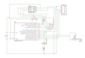
So here we go with KiCAD. It’s new on the block, apparently the thing CERN uses to design their stuff. First thing I noticed is that the workflow is easily laid out in a linear path (which is cool). The second thing I noticed is that they have organized their parts in an awesome manner. It was quick for me to pick out most parts (without the fab-class library).
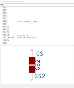
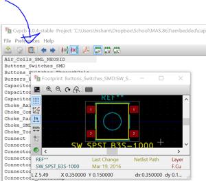
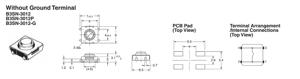
One part I got stuck on was the solder-pad which I would need for the capacitive sensing. I chose the one you see to the left.
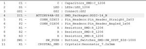
I finished the schematic for the design. This was actually slightly difficult because the process of picking up and moving items was not intuitive / discoverable. The way I did it at first was to use the block selection tool, and carefully select which objects I was going to move. This process turned out to be complete suck.
I read later on the internet that you are supposed to grab objects by pressing “g” and rotate them by pressing “r”. This came in handy when laying out the board.
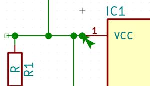
I then ran the error check. It thankfully pointed out where the nets didn’t actually touch the components. This is pretty frustrating across KiCAD and eagle. Essentially, the points in which you connect to components is not well shown in the UI, so it is easy to think you have something connected when you don’t
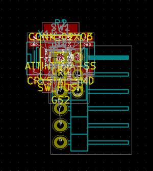
Next came footprint selection. I didn’t use the fab library at first, so I was looking through the library which came with KiCAD. It wasn’t bad. The only issue is there is no live-preview of the footprint that you want to select
In order to get a preview of the footprint for the part you are selecting, it’s necessary to hit the “view footprint” button. This is tiresome for multiple parts
In order to pick out the right parts (wihtout the fab library), I went to digi-key to cross-reference the footprint of the component in the data-sheet. This was an utter waste of time, since the fab class had a library available already (under the tutorials section).
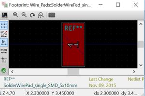
This was the pad I decided to use for the capacitive sensor. It is wide enough that you can get a lot of contact with a finger.

Next came board layout. One advantage KiCAD has over Eagle is that the rats nest is calculated live. This makes layout easier since you can quickly figure out different configurations of your components. Super important if you have a single sided board. I wonder if there is a way to prove whether a circuit can be completed on a single-sided board without zero-ohm resistors? Soudns like a topology problem?
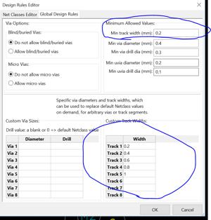
Setting up the track width was absolutely necessary, since the milling tool has a certain kerf. If the traces are too thin, they won’t show up (eaten straight through). So there’s that. You can change these in KiCad through the design rules editor. I failed to figure out how to establis the clearance rules (rules for the distance between components, etc…)
I activated the auto-routing feature, which took care of most of the routes that were necessary. There were a few stragglers, but that’s when I hit a wall.
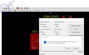
So in order to switch between schematic and board, one must export the nets from the schematic and import them to the board. The problem with doing so, is that KiCAD doesn’t automatically remove old components / wiring (not in a way I could figure out). This is terrible because it means that if I want to put in a few zero-ohm resistors to route some of the hard-to-reach traces, it would require a lot of back and forth work. Lame.
This is when I gave up on KiCAD and switched to Eagle, which, as far as I can tell does everything that KiCAD does, and makes switching between boards and schematics easy.
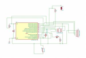
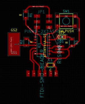
Here’s the schematic done in Eagle. It’s so much faster in Eagle <15 minutes. Maybe that’s due to my familiarity, so I’ll be curious what other people in the class have to say.
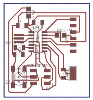
Layout is also easy, and the design-rules can easily be checked. I used 16 mil traces with a 16 mil clearance. I routed things by hand, because I’m a boss. Haha, actually just because i find it fun. I should have used wider clearance, however, since the board came out with areas that couldn’t be milled.
The electronics are all mounted on the top-side. The bottom layer (blue) is the cutout of the board.
I exported this to a png with a dpi of 1500x1500. I figure I could waste the transistors / memory sectors
I worked with Pranam to find out that there was an issue with exporting the png’s on a mac. The mill server will read the image as the wrong size, resulting in the mill building a board that’s wayyy to large.
Luckily I use windows :)
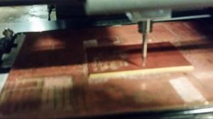
I messed up the milling step a lot. The first time, I ended up placing the mill too low in jog-mode, and having the mill plunge the bit deep into the board, destroying it. When I fixed this issue, I forgot to invert my design, so my board came out wrong. Luckily I had enough board space left over to mill the final board correctly. In the process I figured out a better system to teach the mill:
1) turn on the mill
2) turn on view mode
3) place the bit as deep as you can into the mill with the alan wrench
4) turn off view mode, start up the mill server
5) navigate to the mill website
6) adjust the x and y origin, and hit jog to origin. Make sure this lines up with the bottom left corner of your board.
7) make sure the mill is at least higher than the jog-height over the board (2mm for example). Bring the mill down so that it has room to travel up and down.
8) click “move to origin”. This will lower the mill to the drilling distance
9) Loosen the set-screw, and gently let the bit lower until it is touching the board. Tighten teh screw
10) hit calculate on your design
11) hit send to printer
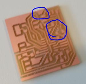
The final milled board. Notice how ther are areas where the clearance was not enough. Next time I’ll use 18 - 20 mills as my clearance. I fixed those issues by taking a utility blade to the overhang regions.
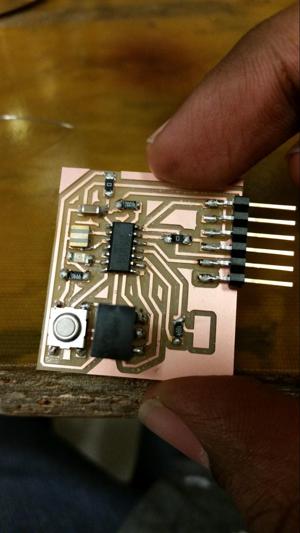
And finally populating the board. You can see the area you are supposed to touch with your finger on the bottom right. I haven’t tested the board out yet, but hopefully it will work wiht the programmer during the embedded programming week.