--How to Make (Almost) Anything--
--Week 03--
--Electronics Production--
--Step 1: Milling the PCB Board
The first thing that was done for this step was to attend a milling tutorial for the Roland machine, and here is where we gained insights on the workings of this machine. A few things needed to be done manually (and I wondered whether the machine was capable of edge detection to streamline the process - however, I digress). The important things to ensure were that the boards were essentially flat on the platform, because otherwise, the milling process will end up crappy, or there is a strong possibility, that the fragile end-mill would break. That said, the process takes some getting used to:One point to note was the offset (for the z-axis), which needed to be a little bit higher than the origin value for that axis. The effect of neglecting this is seen in Figure 1 below (scratches on the board as the endmill is dragged across the board when it needs to change locations).
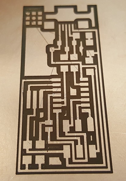
Figure 1: Effect of end-mill dragging on finished PCB board
I made sure that this did not affect the functionality of the board (I used a multimeter to check for continuity, as well as examined the board under a microscope to verifiy that the traces were indeed still intact)
--Step 2: Stuffing the Milled PCB Board
This process essentially involved looking at the component layout, as depicted in Figure 2, and then sourcing the associated surface mount components from the inventory in the EECS lab. When all the the components were sourced, I began soldering components one-by-one, by first tacking the component being soldered on one side, and then soldering the remaining legs to the board.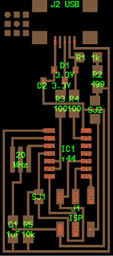
Figure 2: Component Layout
In retrospect, I should not have started with the USB component, as this was one with the thinnest distances between pins. I followed Neil's advice on the matter, by first putting a blob of solder across all the pins, and then "attempted" (the key word) to remove the solder between bins, by way of a solder-wick. This "attempt" proved to be a disaster! Considering that I have an EE background, this was painful to watch. That said, I ended-up consulting with Gavin, who showed me the trusty electric solder sucker. This ended up cleaning up some of the solder mess that the solder wick left behind. I tested for contunity and possible shorts, and the joints checked-out fine.
I then proceeded to solder the rest of the components onto the board, checking for continuity and possible shorts, after each component was stuffed on the board, and the finished product is depicted in Figure 3 below.
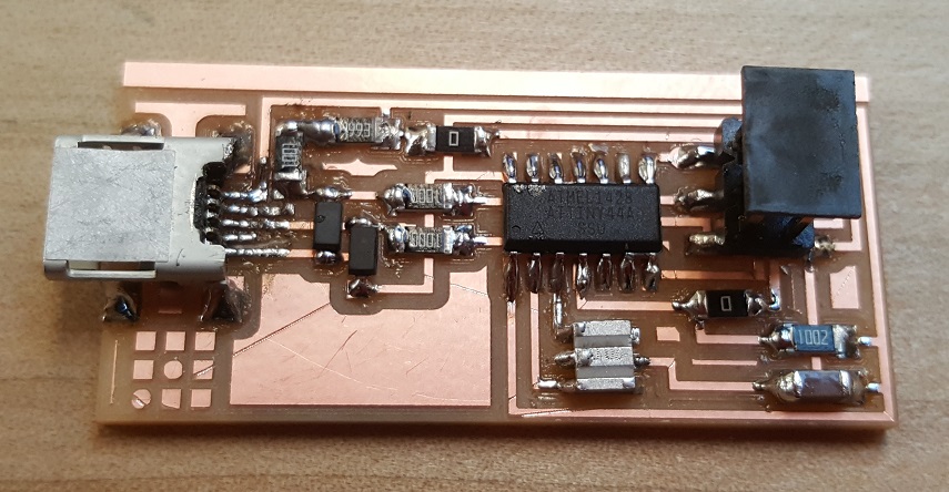
Figure 3: Finished Board
--Step 3: Programming the PCB Board
It would have been nice for this to have been the last step, but unfortunately this is not the case. The step seemed pretty straight forward, as I intended to initially use the lab computers, already set up with the programming interface, and connected with the programmer, and then after successfully programming and checking that my programmer was being recognized as a USB device - this last segment of USB recognition is where everything pretty much halted: it was not recognized, and I was certain I had all my i's dotted and t's crossed (checking every step of the way, to make sure nothing was shorted, as I soldered, and ensuring that connections were made properly). Figure 4 depicts the step where my programmer failed to be recognized.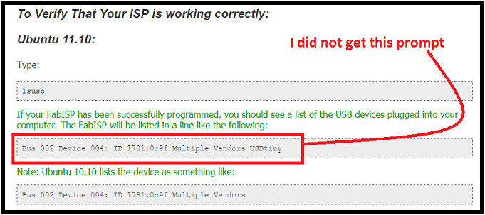
Figure 3: Failed USB Recognition
TROUBLESHOOTING: I took the following steps to sanity check my board for defects
- Checked all the traces and all the connections again for continuity and shorts.
- Checked diodes D1 and D2 to ensure that they were oriented in the right polarity.
- Checked the drop across the diodes to ensure that they were indeed functioning properly.
- Checked the 20MHz resonator on an oscilloscope, to ensure that it was indeed pushing out 20MHz when power was applied.
--Step 4: Refabricating a new board!
For this process I stepped through Steps 1 through 3 again, but this time I chose the board which had the 2 pin oscillator supported by two additional 10pF capacitors on each side (the first time around, I chose the 3 pin resonator board design merely because it had less components to stuff onto the board). Figure 4 shows the component layout for the new board, Figure 5 shows the finished board after milling, Figure 6 shows the board after being stuffed with the required components, and Figure 7 shows the successful recognition of the newly fabricated board after programming. At this point, what was left to do was to take off the 0 ohm resistors SJ1 and SJ2, in order to commission this new board as a programmer.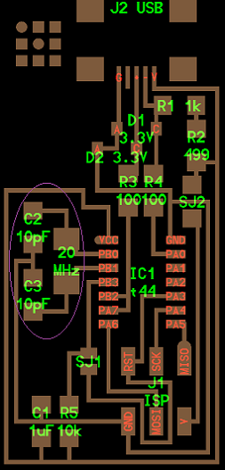
Figure 4: Component layout for the new board
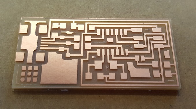
Figure 5: New board, after the milling process
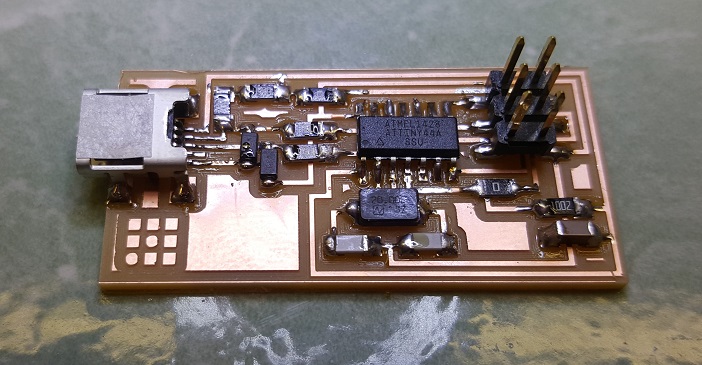
Figure 6: New board, after the stuffing process
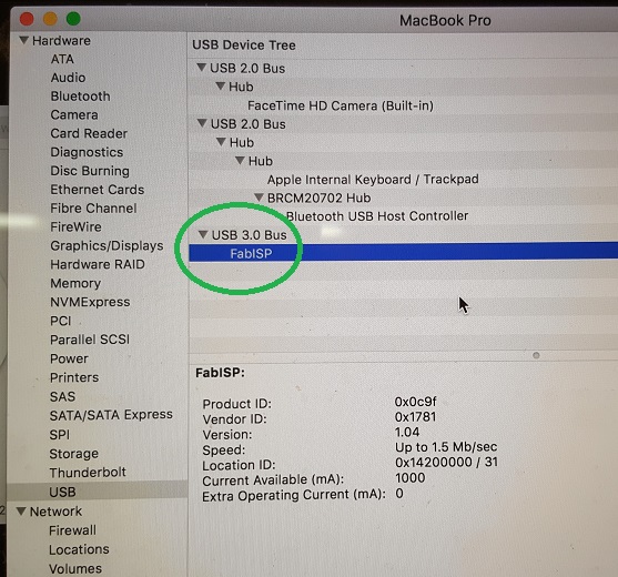
Figure 7: New board - Successful programming and USB recognition!
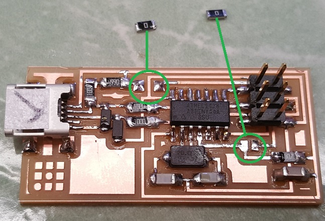
Figure 8: New board - 0 Ohm Resistors removed
--I should point out a few things here
- In hind sight, one thing I would elect doing to make this process a little smoother, is to put some sort of an indicator (perhaps an LED), to show a few things (at least, indicating that the board is powered on, for starters)
- I would have also milled the same board with the 3 pin resonator a second time (and I still intend on doing this), for a sanity check, that the components were not the issue.
- I would ensure that I have all the components for the board available, before committing to a board design. Because at some point during my stuffing of board 1, I ran into an issue of having the wrong 20Mhz resonator for my board, as depicted in Figure 9.
- The re-fabrication process for the new board serves as a reassurance to me that I have not lost my PCB fabrication skills from my EE days - I'm still an engineer, dammit!
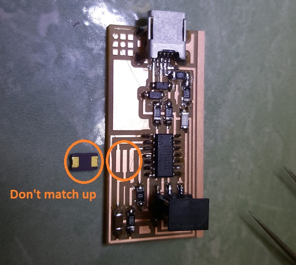
Figure 9: Wrong resonator for my first board
Figure 10 depicts the two boards side to side - the check mark indicates the working board.
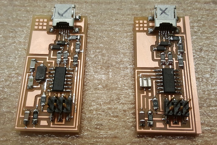
Figure 10: Both boards side by side
Fun project! I'm looking forward to using my new programmer to program my custom designed boards for subsequent projects.