--How to Make (Almost) Anything--
--Week 05--
--Electronics Design--
--Step 1: Designing the board in software
I found this step to be straight forward, as I have a background in electrical engineering. So the point of contention was essentially which software package to use - either KiCad or EAGLE. I am more familiar with EAGLE, because I have used it in the past, so in the interest of time, I decided to use this.I selected the library file from the Fab website, and included it within the path of other libraries that EAGLE typically comes with. I referenced the "board" file on the website to identify what components I needed to select connect for the board. Also, aside from the initial board, we had a requirement to add at least a switch and an LED to the board and hook them up to free pins on the IC. This essentially, was a matter of looking up the pin layouts for the switch and then connecting them accordingly. The final board design is depicted in Figure 1 below.
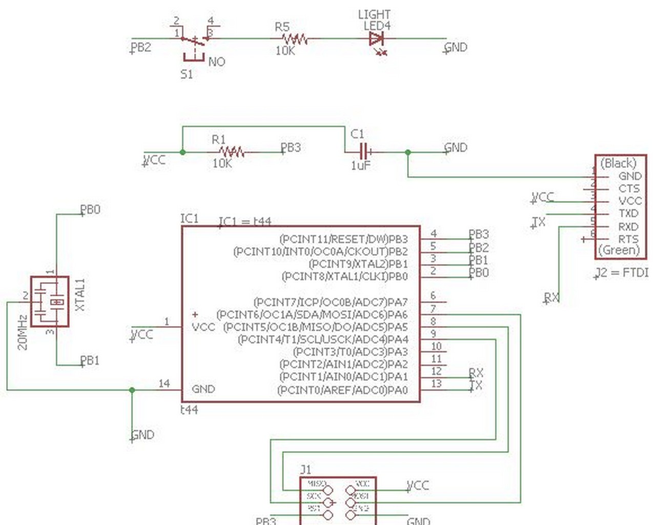
Figure 1: Final Board Design
--Step 2: Connecting the traces in software
I typically lean towards hand routing traces whenever possible, and this board was small enough for me to reasonably do that, in addition to the reference from the original board design that was available from the Fab website. I used a 0.016 width for the traces and ran it through the DRC (Design Rule Check) after all the traces were laid out, to make sure that the trace layouts were within the tolerances specified in the DRC document - and it checked out alright. I then used the outline layer to draw the boarders for the board layout. I exported the images from this "trace view" to a PNG format, with a resolution of 1000px (because upon checking the 500px default setting from EAGLE was quite grainy upon review). The first image exported was just of the traces, i.e. with the outline layer hidden; and the second export was just of the outline, i.e. with the trace "top" layer hidden (this second export serves as the "interior" or border of the board to be fed into the SRM-20 milling machine control interface). The traces and outline are depicted in the following Figure 2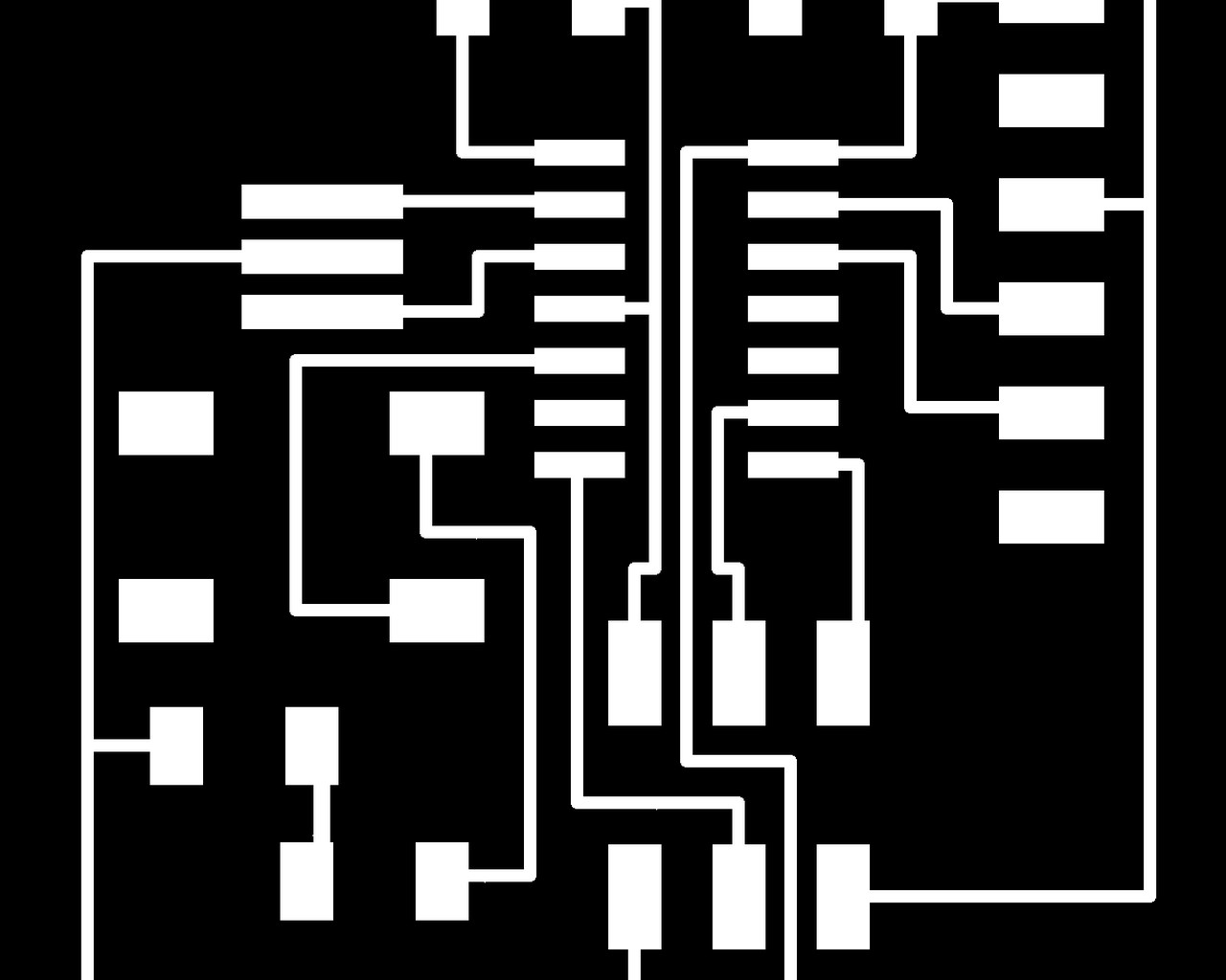

Figure 2: Traces and outline for the board
--Step 3: Board Fabrication
This step involved a lot of what we already discussed in the "electronics production" lab week, so I will spare some of the details of loading the PNG, and cutting the traces, and move right to the outcome of the boards. One thing that stood out initially from the board, when the traces were milled, was that the three traces which ran through the IC were fused together, despite it checking out OK on the DRC check in EAGLE. This is depicted in Figure 3 below.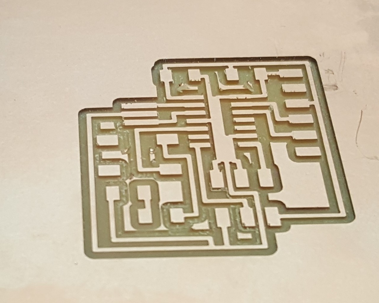
Figure 3: Fused traces on the milled board
But my intention was to just use an exacto-knife, or a similar tool, to separate the traces, so I moved on to the step in the milling process for cutting out the interior. This proved to be a disaster for one key reason. The mill-end drove right into the board and cut out the board, the "sacrificial" board, and engraved the wax surface below: take a look at Figure 4 for a better illustration. What actually occured was that even after changing the mill end to the 1/32 for the interior milling process, and the jogging the z-axis to the new location, I then entered the new location for the z-axis in the "move to home" section, but never actually clicked the "move to home" button, and it quickly became apparent that this step (clicking "move to home") registers the new location in memory, but this did not happen here. The board was compeletely ruined. Yikes, won't do that again!
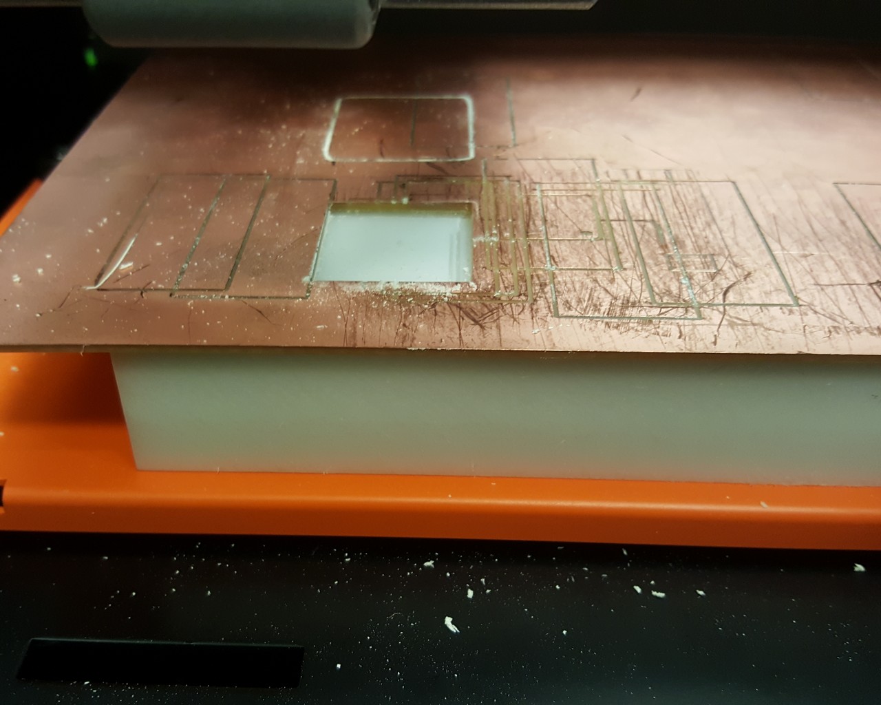
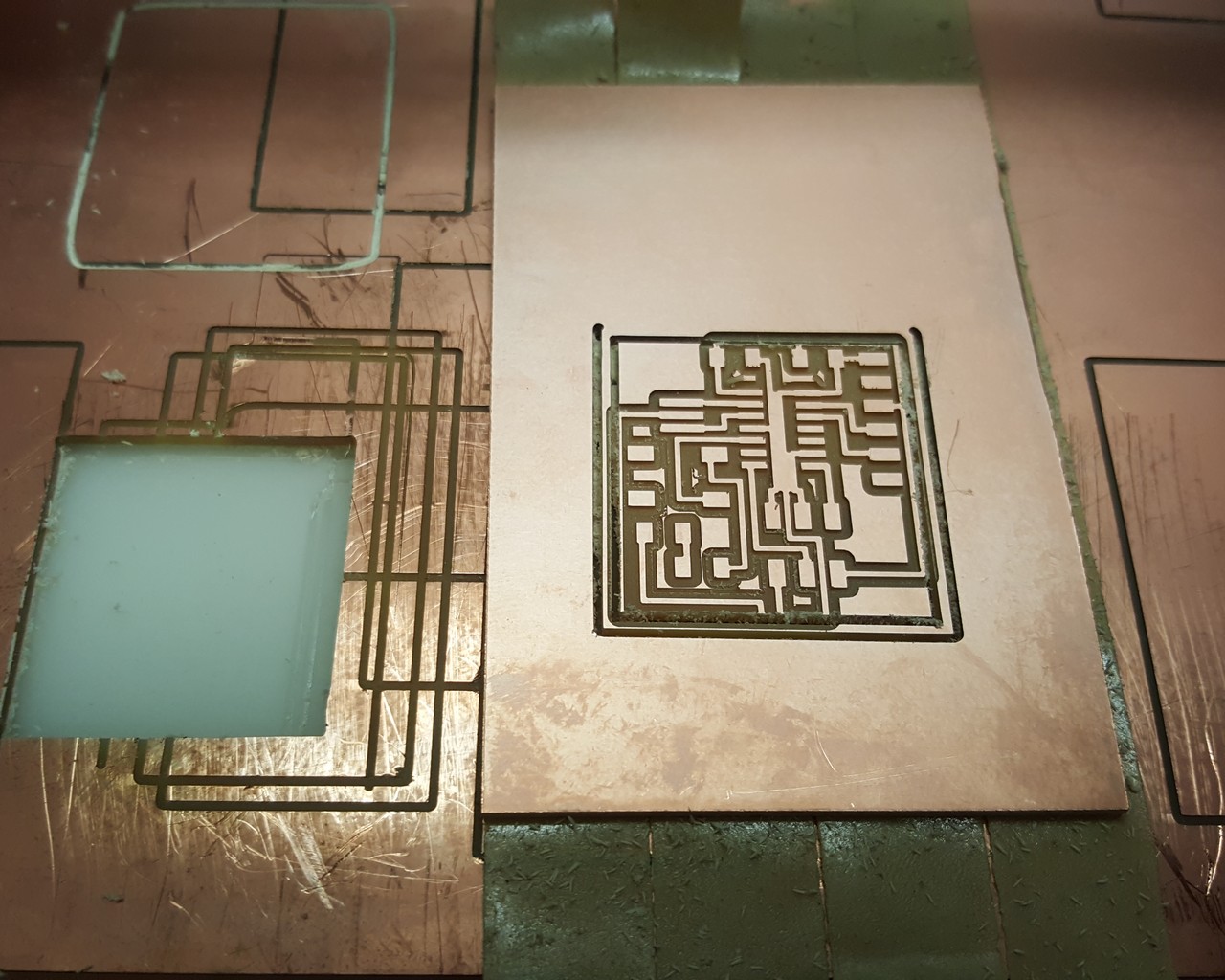
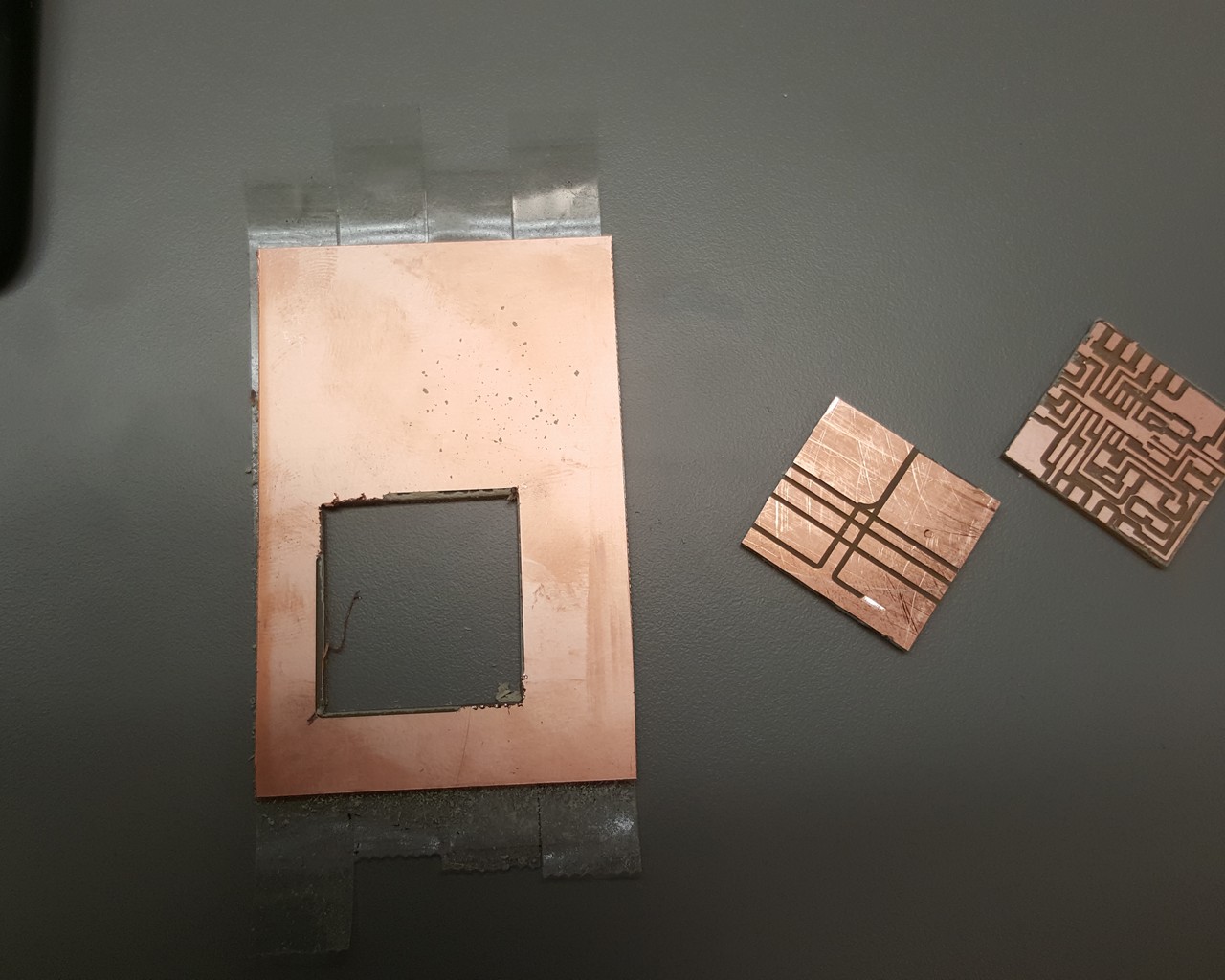
Figure 4: Cut too deep on the interior milling
--Step 4: Retracing and Refabricating
Considering that my board was now ruined, I moved on to redesigning the traces to have a smaller width of 0.012, in order to avoid the fusing from happening again on the new board (I also made sure to view the tool path to ensure that 3 individual traces would be the outcome in that segment). Everything checked out here, as shown in Figure 5 below. I then went on to milling the "interior", with this new found caution from my last attempt, and it milled out great - as depicted in Figure 6 below.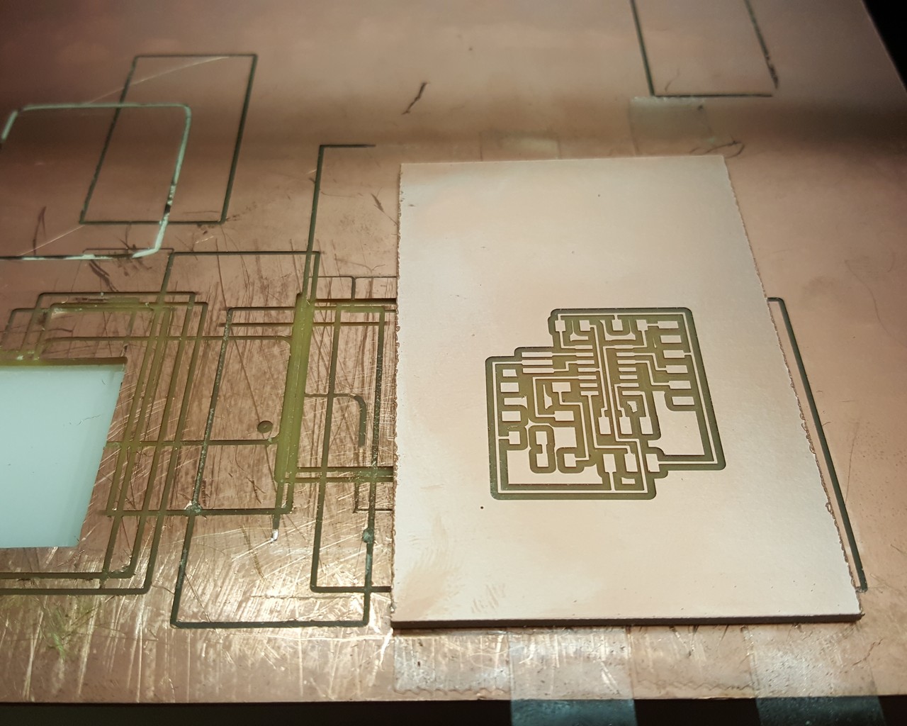
Figure 5: Traces on the milled board no longer fused
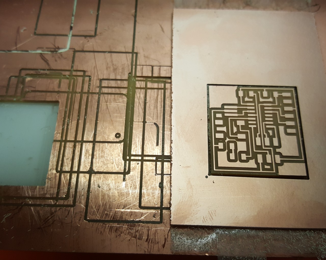
Figure 6: Second attempt at milling out the entire board was a success
--Step 5: Stuffing the board
After the board was milled out, I sourced the individual components which made up the board, and then soldered them onto the board - the final product is depicted in Figure 7 below, however, this board is yet to be programmed and tested. Also, I need to refabricate this board because, the 6-pin connector on the edge of the board does not have a proper resting surface, so the solder is load bearing at this point (not good!).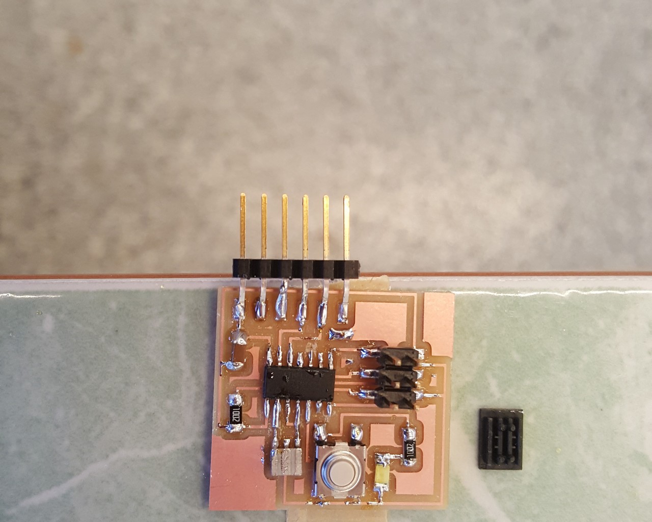
Figure 7: Final stuffed board