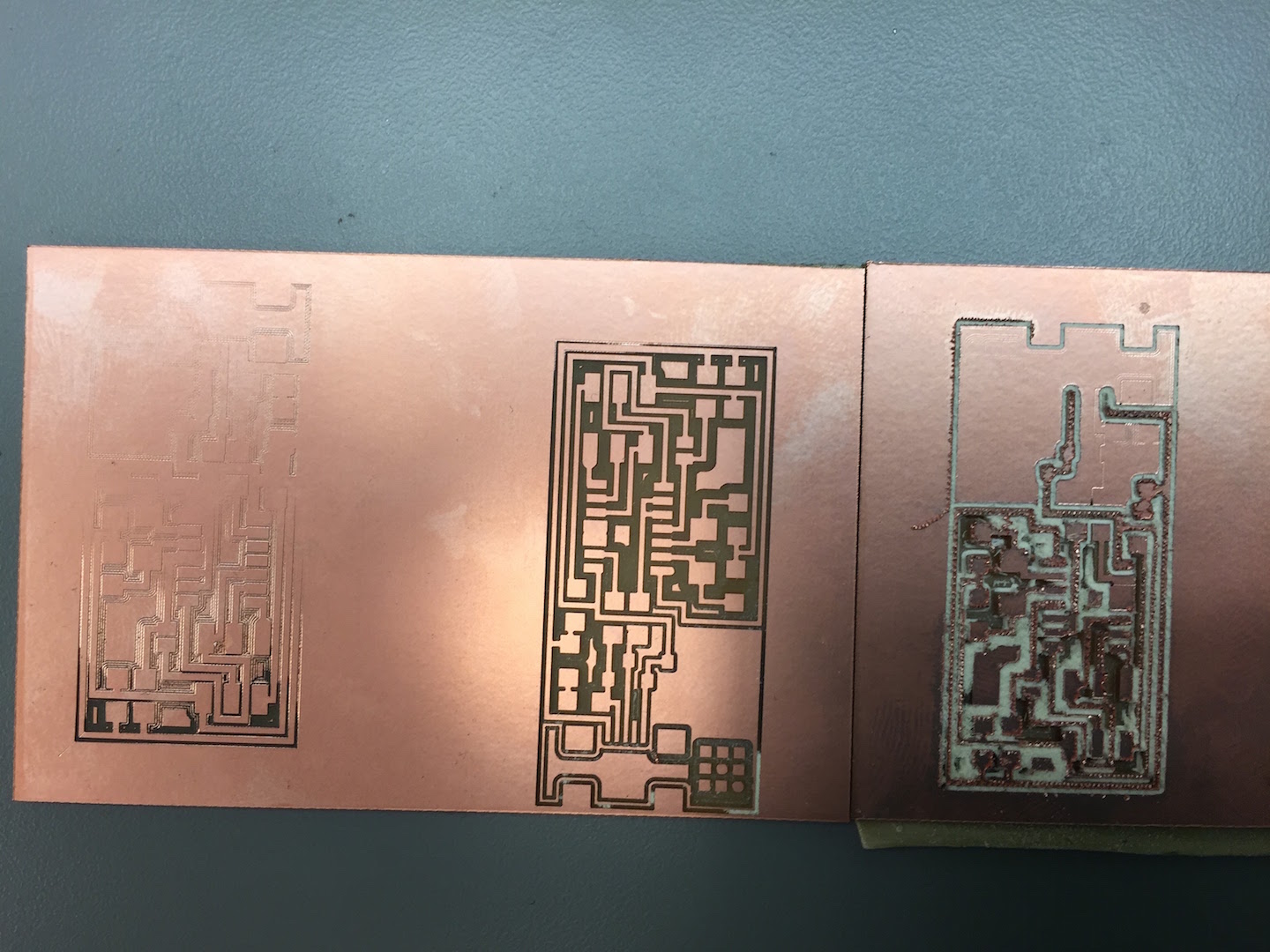
It seemed like a straighforward, 10-minute job: Taping the board, screwing in the end mills, and calculating the origin coordinates. NOT SO. Three circuit boards and 1.5 hours later, I finally had a product on which to solder the electrical components.
Lessons learned:
- When preparing to print, raise the Z coordinate to screw in the end mill. Then, lower the Z coordinate and release the end mill so that the tip of the end mill taps the surface of the board. The tip should rest snugly on the board to create visible traces without cutting through the board.
- When adjusting the coordinates, calculate and eyeball the position of the mill to prevent off-roading. During my second attempt, the end mill started tracing a few millimeters further from the border, resulting in an off-center print. Since I was unsure whether the traces would fit onto the board, I canceled the job and re-started on a fresh one. This time, I raised the Z coordinate for "Jog to Origin" to increase the elevation of the end mill when lifting and shifting, thus preventing surface scratches. By setting precise origin coordinates and verifying the end mill position with a visual scan, I completed the PCB milling.
Step 1: Load the traces and interior files for printing. Set and calculate origins for the end mill.
Step 2: Send files to print, switching from 1/64 to 1/32 for the end mill to create the traces and interior, respectively.
Step 3: Practice to make perfect: Adjust and tighten the end mill to print at the right depth. Re-calculate origins to center traces on the board and ensure space for the interior. Origins on the final attempt: x=110, y=10, z=5, where jog to origin was z=10.
Step 4: Feel accomplished for deceptively simple project.

