Since this is my first time using PCB design software, I installed KiCad, as I understood it to be the most intuitive product. However, after discovering the Fab.lbr file in the class tutorials, I switched to Eagle since I could create a directory of components: Prior to this breakthrough, I had been struggling to match the components from the Hello Board design to those in the pre-packaged libraries, both in Eagle and KiCad. Each component seemed to have an endless number of packaging variations! But I got the hang of it as I surfed between the Hello Board design, the manufacturing descriptions for the parts, and the component libraries.
Getting the library right was a critical step to completing my design, which consisted of a schematic and board layout. And while I am averse to YouTube videos, YouTube tutorials became my best friend over this glorious Columbus Day weekend - I had so much SparkFun (pun intended) and recordings by this Jeremy Blum Eagle pro.
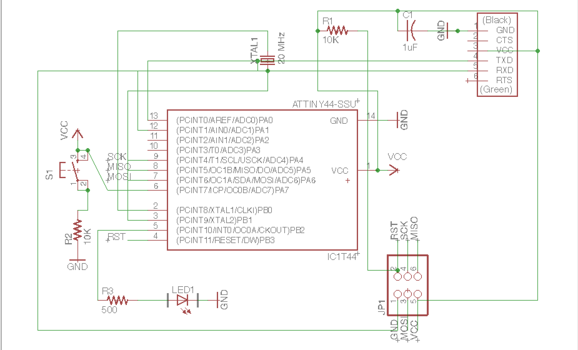
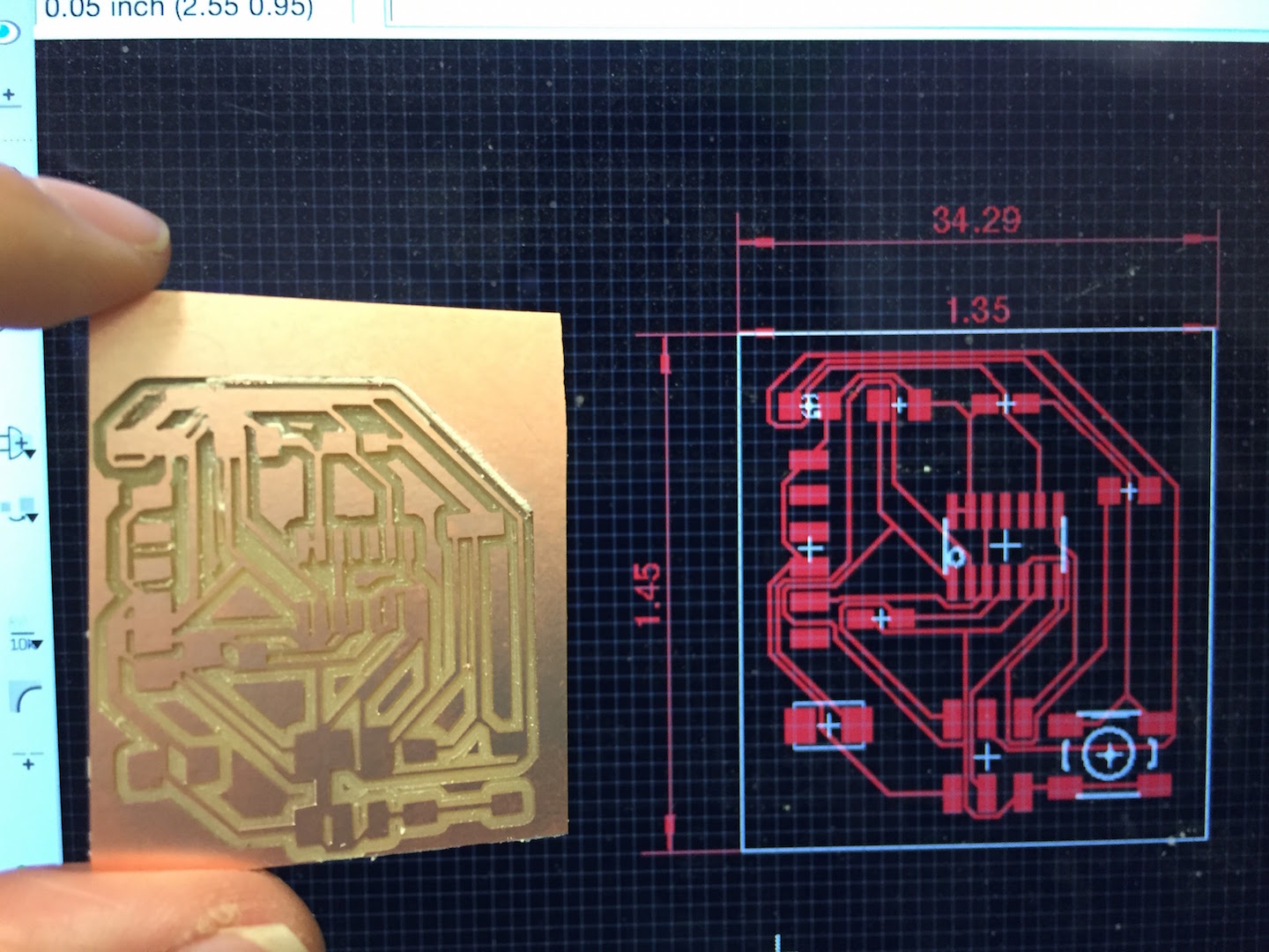
To create the schematic, I selected all the components from the Fab and Eagle libraries. To customize my design, I added a switch and LED. Then, I connected the components with nets and junctions, which simulate wires. I learned the fundamentals of PCB design: naming / labeling components, ascribing values to parts (e.g. resistor 10K), and adding supply sources, such as voltages and grounds. As for labeling, I realized that labeling nodes on the program header and IC1 would create electrical connections without a wire illustration. Pretty cool! Once I finished the schematic, I used it to create a board layout.
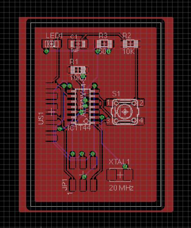
To build the board layout, I used the Ratsnest function to arrange the components within a perimeter. Then, I edited the Net Classes to determine trace width, drill, and clearance. Next, I used the AutoRouter function to optimize the traces. Initially, I made a mistake and enabled Eagle to optimize routes for the top and bottom layers of copper. However, a peer offered some pointers, and I adjusted it to optimize routes for the TOP Layer ONLY. Several times, I needed to re-arrange the components and re-instigate AutoRouter because there were airwires: Airwires flag traces that won't work on the circuit, and in my design, most were due to excessive cross-overs. But, I finally got it right, and I verified the design was 100% good-to-go with the Design Rules Check (DRC)
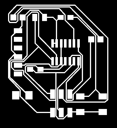
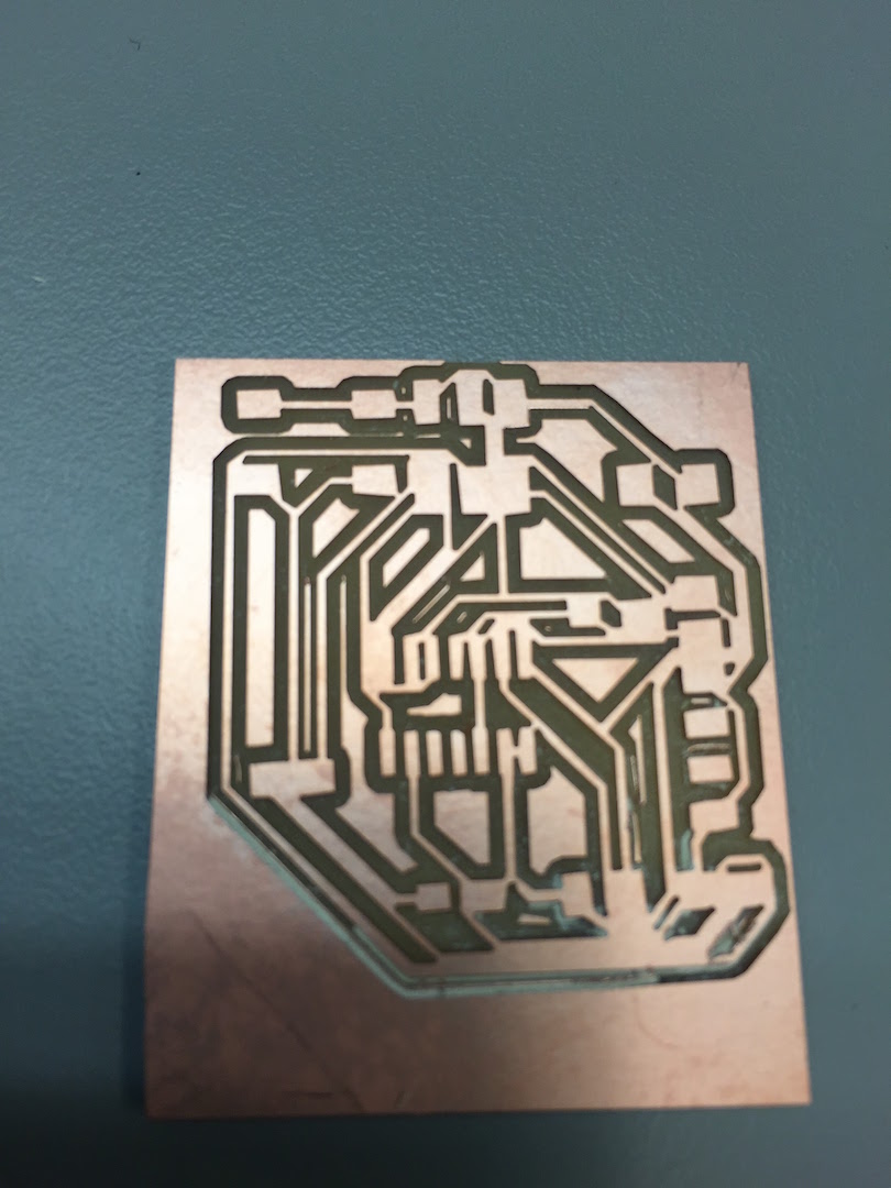
To wrap up the design, I exported the board layout as two images: traces and outline. I modified the layers in order to create a file that could be loaded into the PCB Mill. For the traces, I checked off "Top", and for the outline, I checked off "Dimension" in the View options. When prompted to export these files, I checked off "Monochromatic" to emulate the designs from our Electronics Production week.