Week 4: Electronics Design
My Version of Echo Hello-world Board
Oct 12, 2016
Assignment
Redraw the echo hello-world board. Add at least a button and a LED. Check design rules and make the board.
Tools used this week: KiCad, Roland SRM-20 PCB Miller.
Echo Hello-world Board
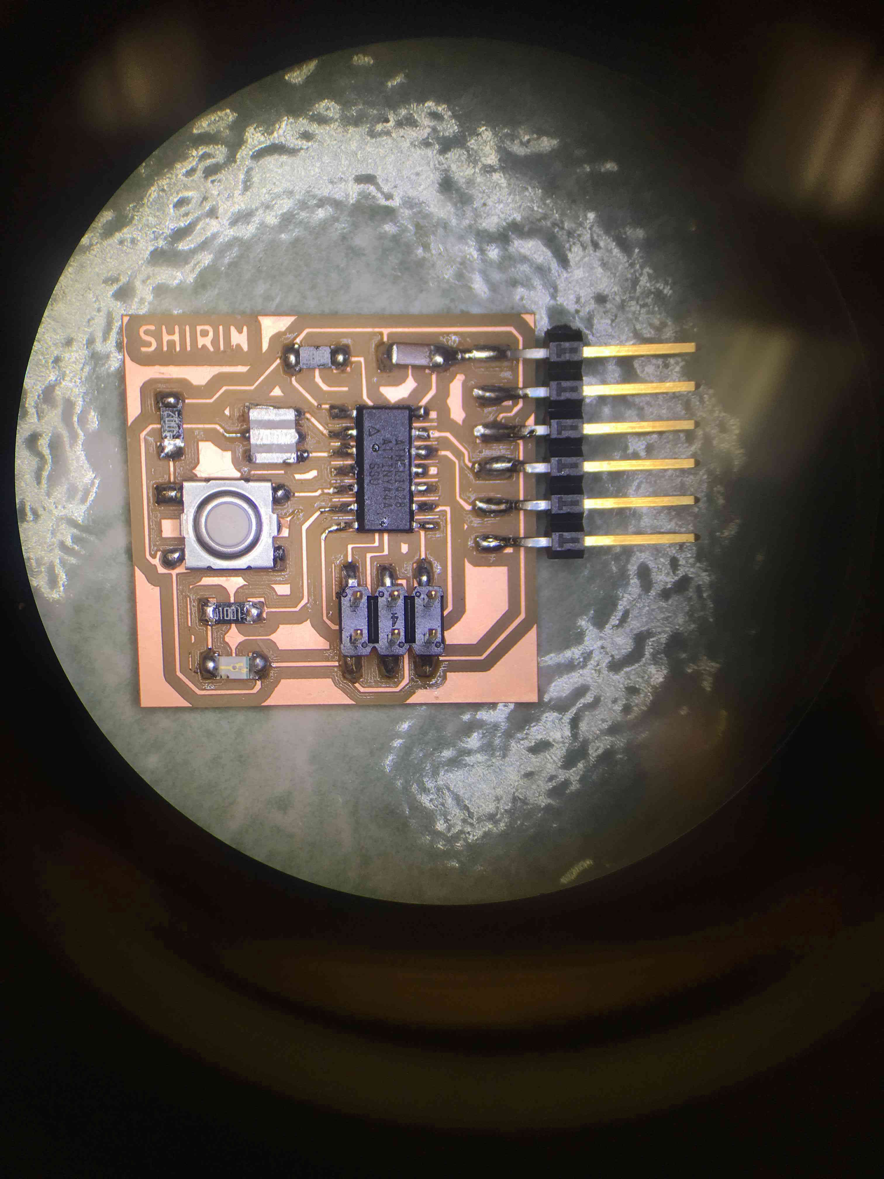
This week, we focused on electronics design. I modified the echo-hello world board based on Neil Greshenfeld's design to include a button and an LED. I've had to deal with the complexity of Altium before in one of my internships. This time, I briefly looked at Eagle, but since its workflow and features seemed similar to Altium (although simpler!), I decided to try KiCad. KiCad is definitely more beginner friendly and simpler to use than Altium for individual work. Since it's an open-source platform, there are still small bugs especially in the graphics UI.
Board Design in KiCad
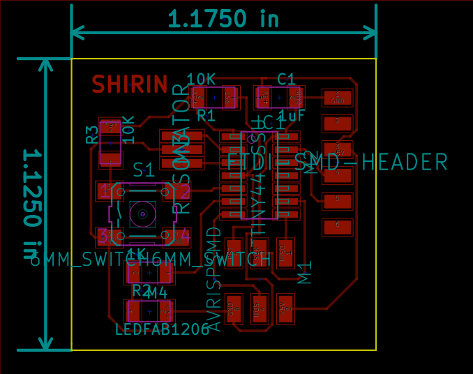
I watched a couple of tutorials to learn Kicad. There was nothing complicated about it, execpt importing libraries. First of all you need two serparate libraries, one for schematics and one for pad layouts. I also had to manually match components in the two libraries, becuase for some reason Kicad didn't recognize the matches.
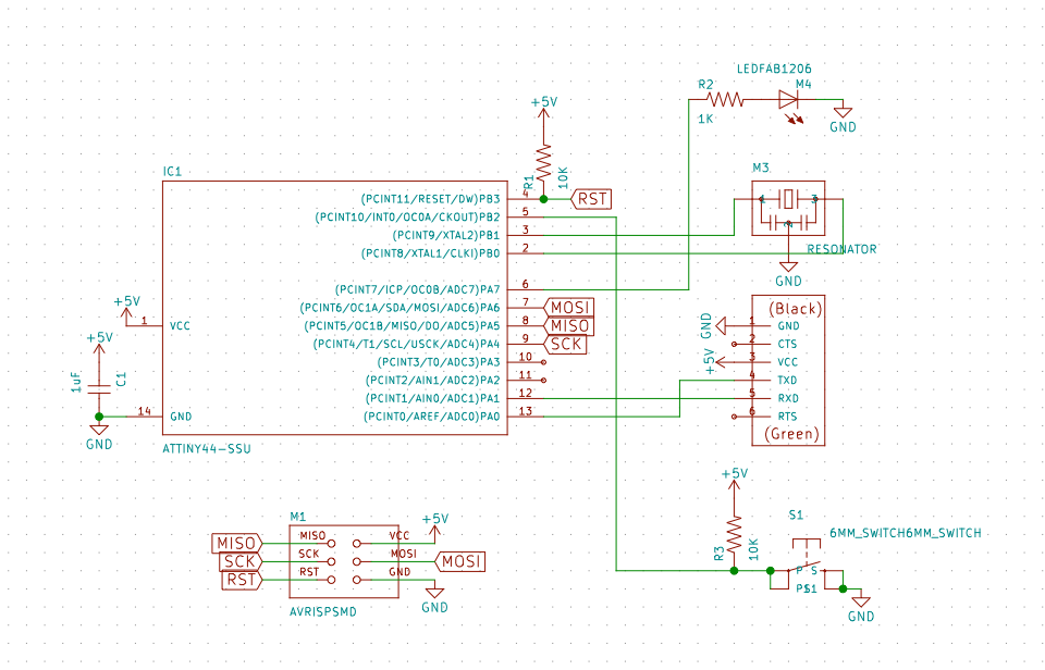
Besides what Neil had on his board, I used two of the GPIO pins and added a button with an external 10K pull-up resistor, and an LED with a 1K resistor, which would draw a 5mA current from the microcontroller pin.
Making the Board
I encountered a number of problems as I was preparing traces for printing. First, I had a really hard time figuring out how to export just the board are and not the entire sheet. I ended up manually cropping the board area in gimp. Second, Kicad doesn't export png and mods reads png only. So every time I exported a board for printing I had to convert from svg to png, which I did in gimp. Then the png file had a transparent background with black traces. What the printer needed was black background with white traces, so I had to manually add background and invert colors (again done in gimp).
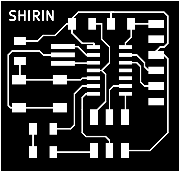
This is before gimp processing:

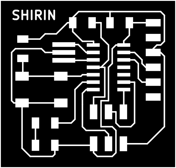
This is post gimp processing:
Lastly, I made sure the image quality was 500 dpi.
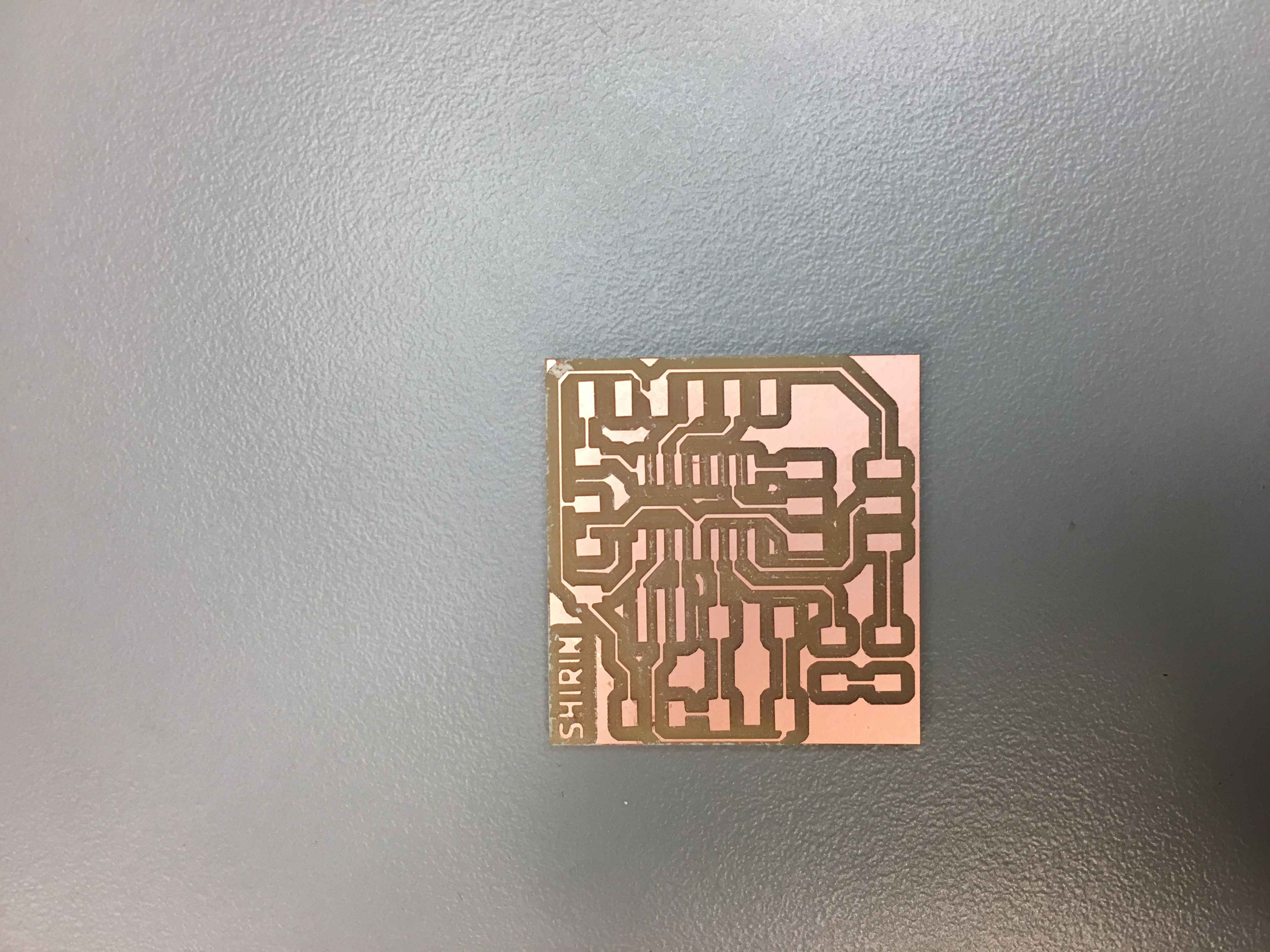
First time I printed the traces and looked at them, I realized something terribly wrong: unconnected ground pins! I was very surprised that DRC didn't catch unconnected pins. Anyways, I went back and fixed it manually.
After printing the board I realized my traces were very narrow, 0.010 inch thickness, with more than enough space between them. When I was soldering, a few of the traces came peeled off of the board easily. I fixed them by addering extra solder on the traces.