
This week I wanted to make a six seven-segment-LED display that could pair up with my color sensor and display the corresponding hex values. I began by doing some research online to see how seven segment led displays work and then began to put together the PCB in Eagle.
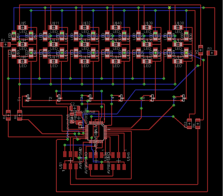
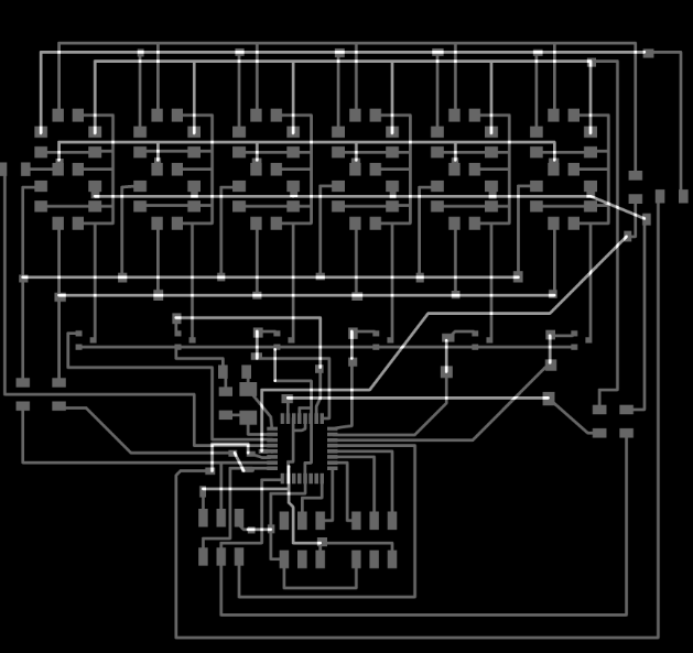
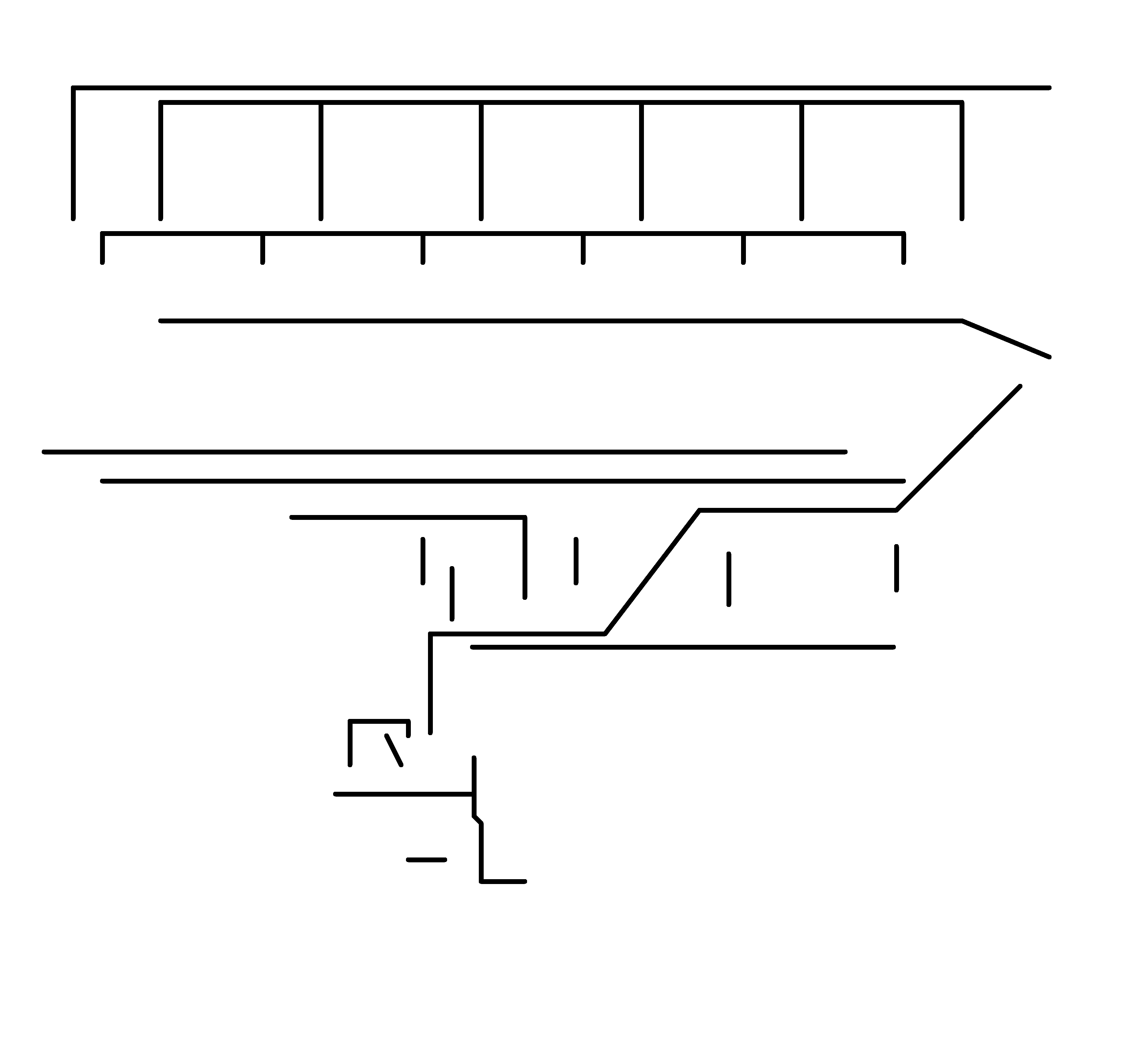
Below is an image of the schematic.
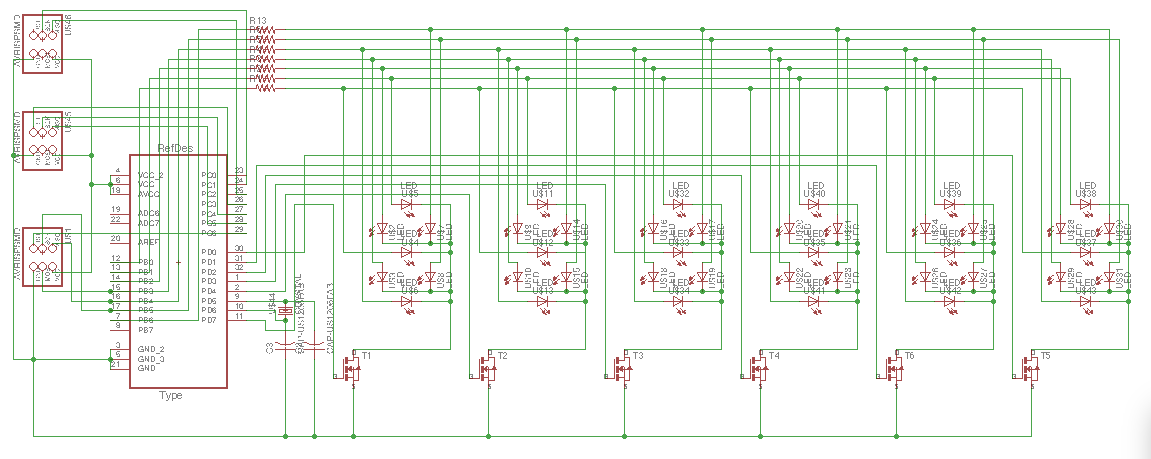
This is a key of the components used:
1) White - LED
2) RED - n_channel mosfet
3) GREEN - resistor (499ohm)
4) BLUE - capacitor (10pF)
5) YELLOW - atmega138P
6) PURPLE - 20MHz Crystal
7) LIGHT BLUE - six pin ISP header.
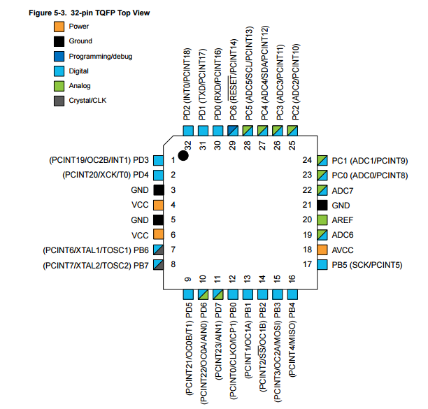
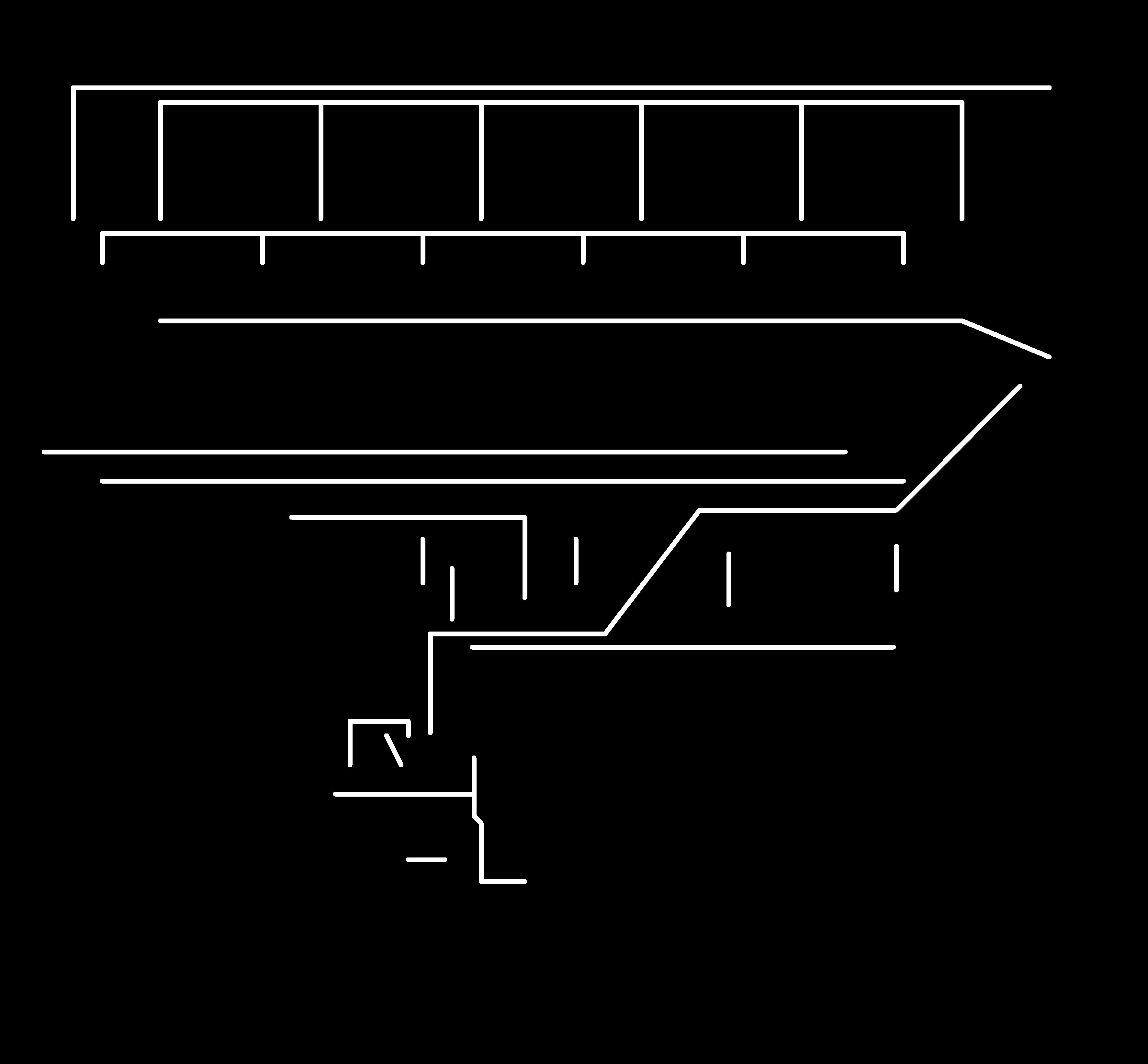
I used the atmega138p microcontroller - the pinout is shown below.
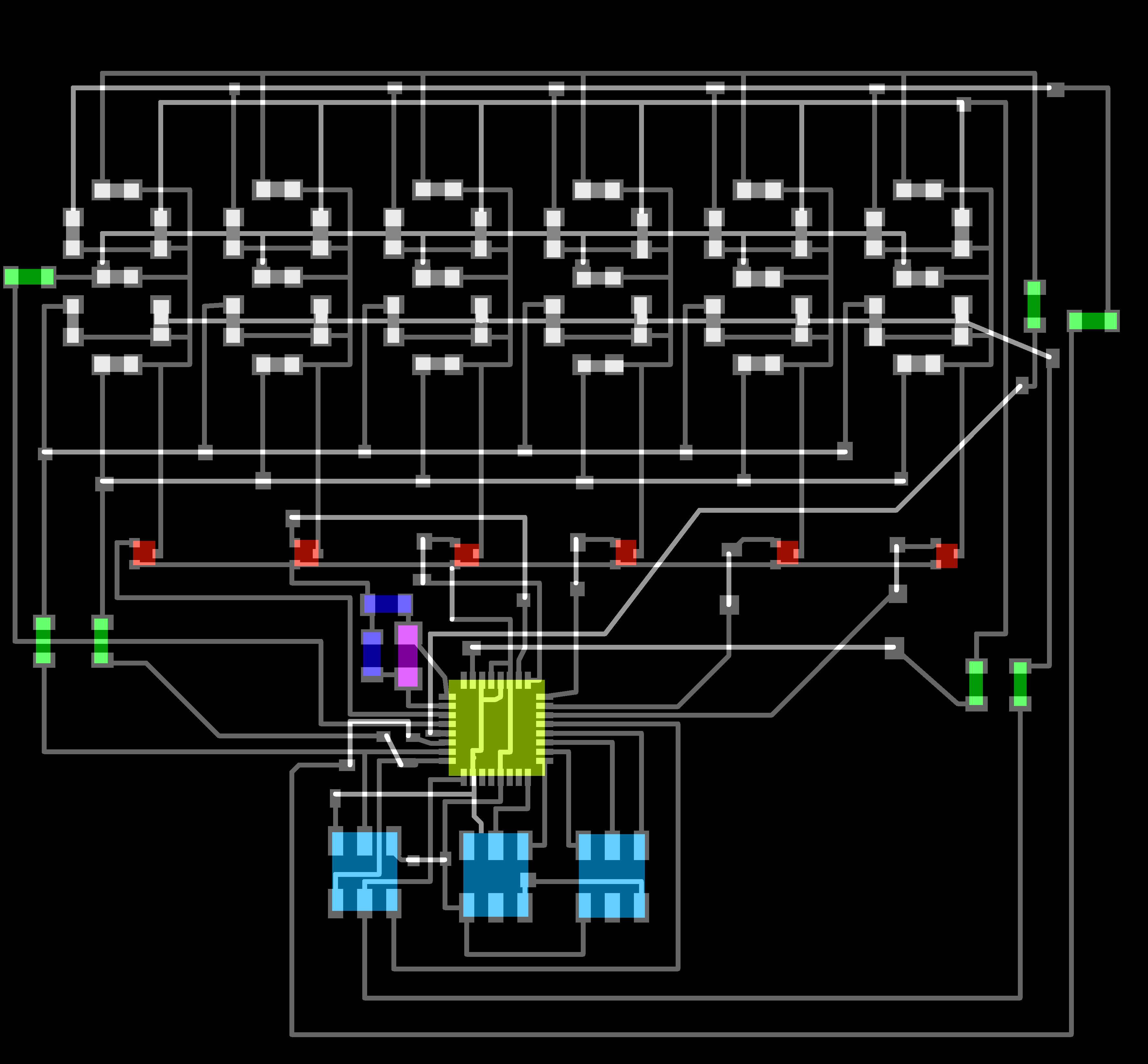
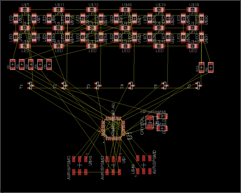
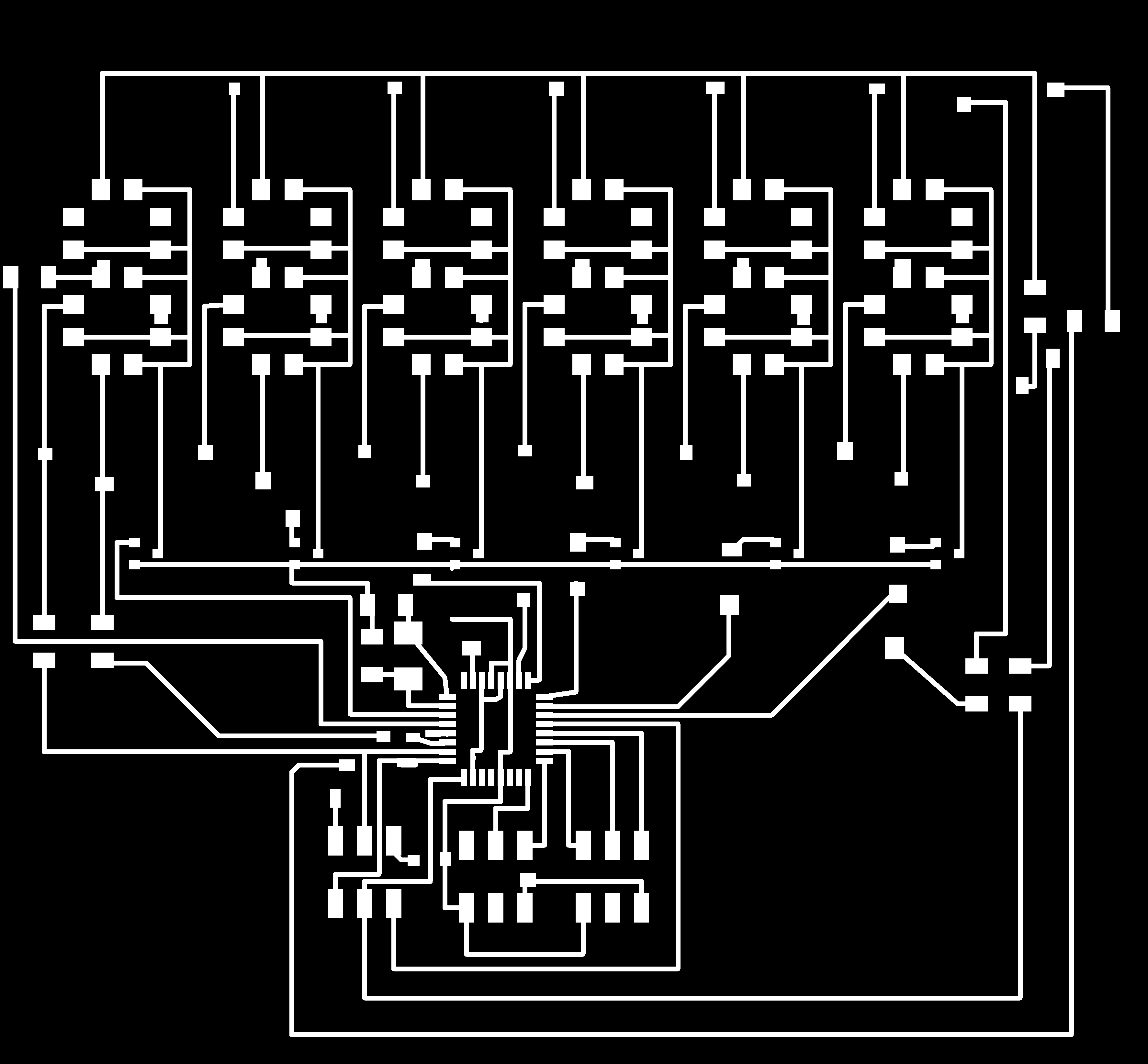
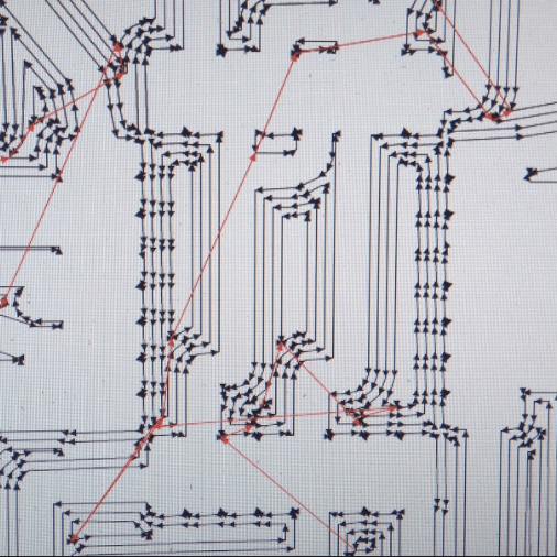
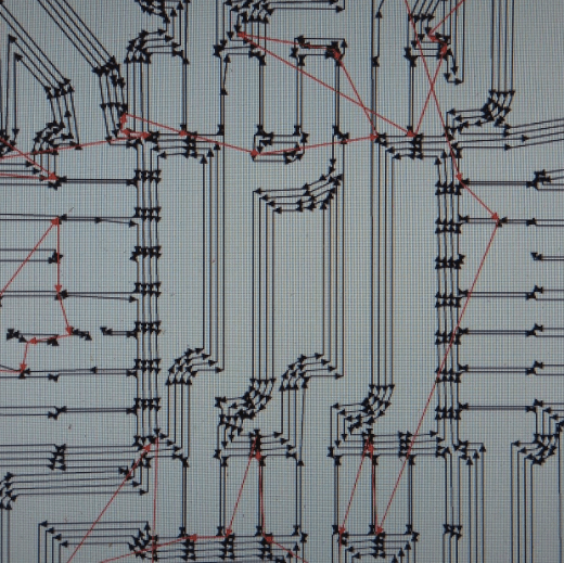
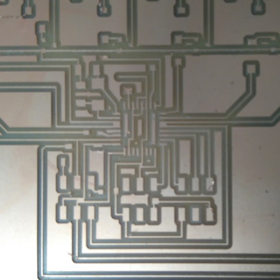
Okay - now for the routing!. I ended up using two layers with vias between them. Instead of milling on both sides of the board I am going to try utilize the epoxy vinyl and copper vinyl...
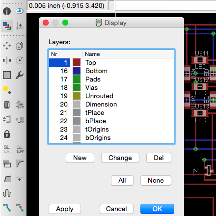
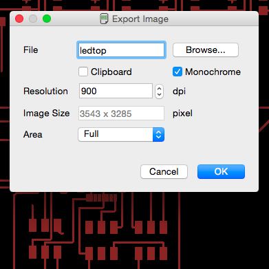
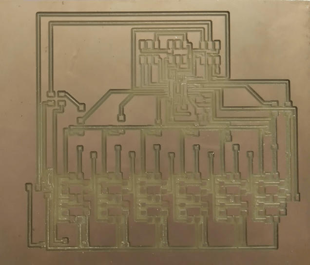
Okay - ALL DONE. Now I use the layers tool to control which layers appear inorder to save the traces on the top separate from those on the bottom as monochrome images. The save options I change to 900dpi so that the resolution is really good.
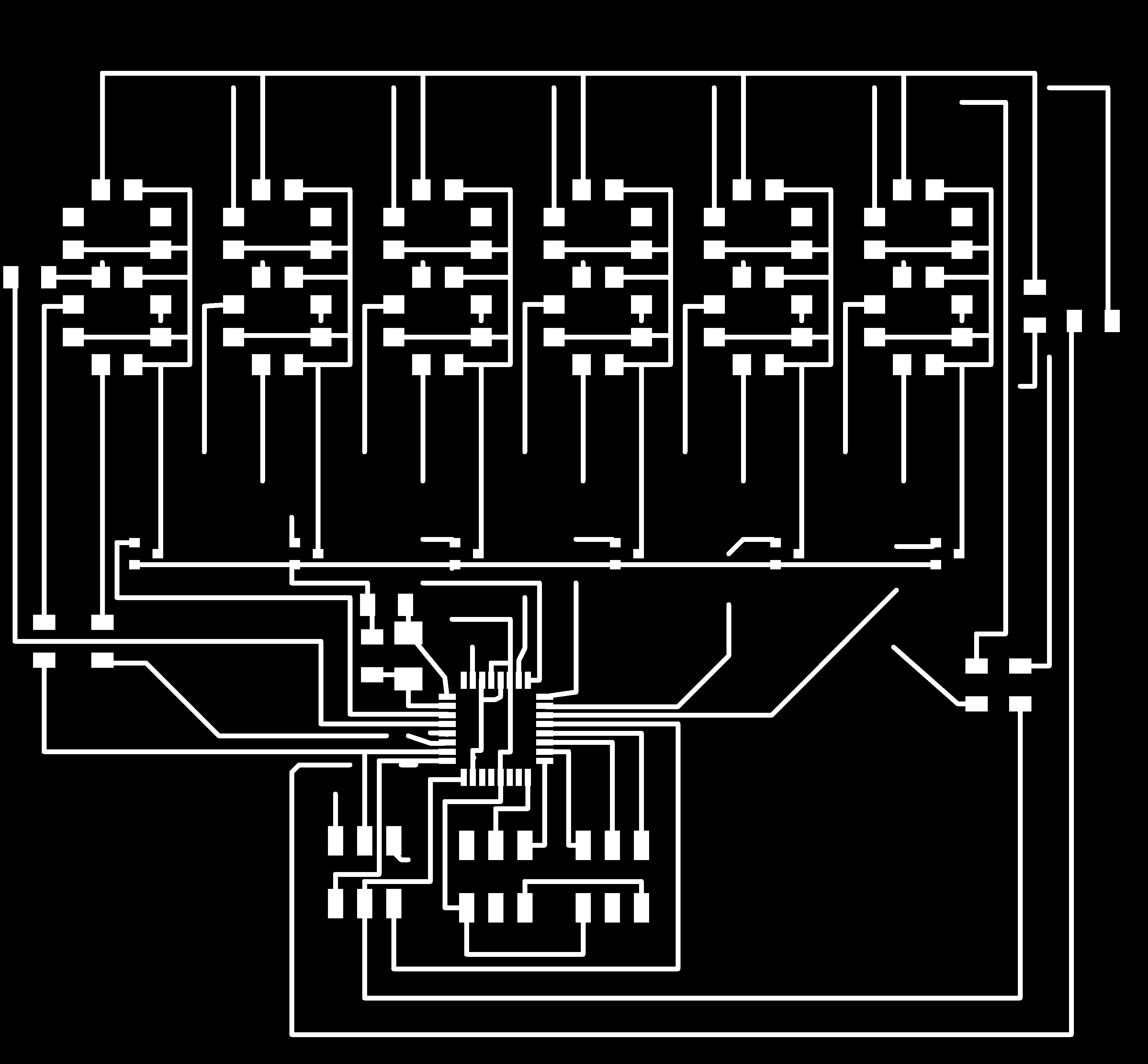
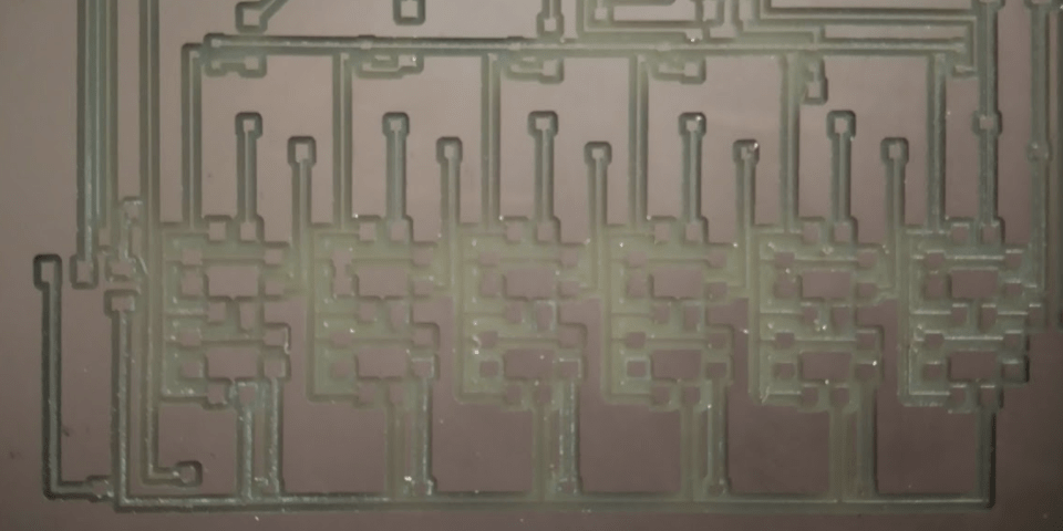
Here are the raw monochrome images.

I uploaded the monochrome images into gimp and saved them to different layers. I then changed the layer opacity to allow me to work with both layers in view. The reason for editing is to create pads on the bottom layer so that the vinyl cut copper layer will be able to connect to it as well as to create a layer for the insulation epoxy vinyl (this will separate the copper vinyl layer from the bottom milled layer)
I reset the opacity to 100% on the layers and then exported the image to png three times each time showing different layers but hiding the ones I did not want.
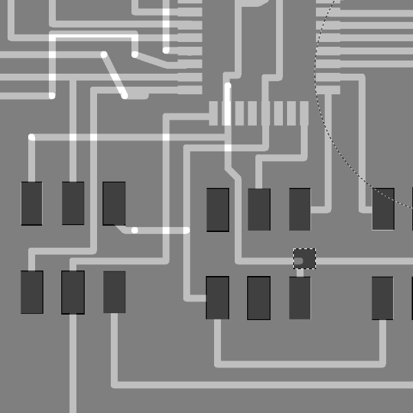
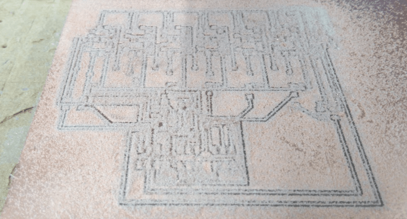
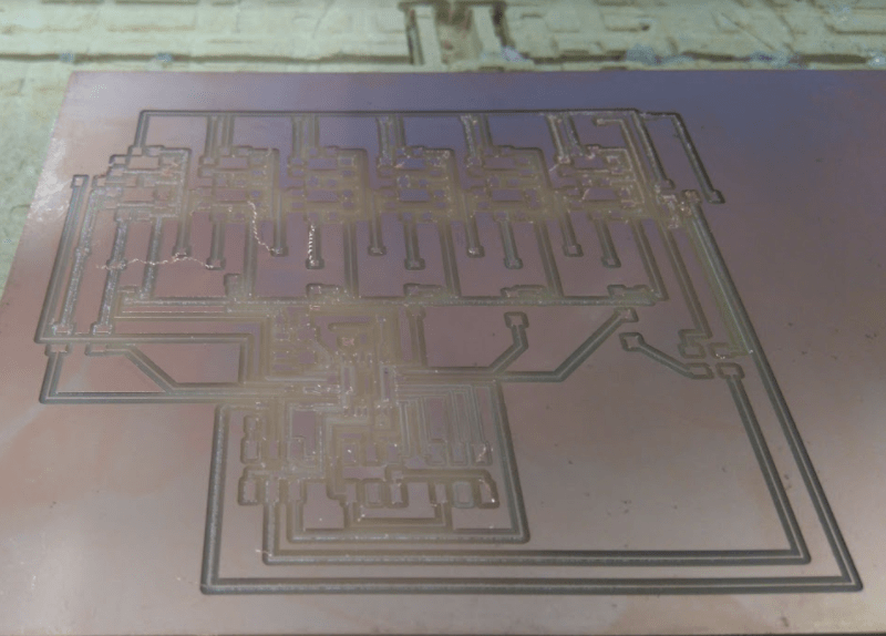
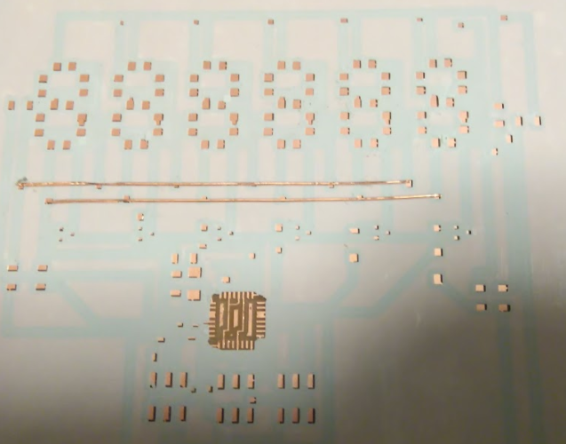
BOTTOM LAYER - milled layer.
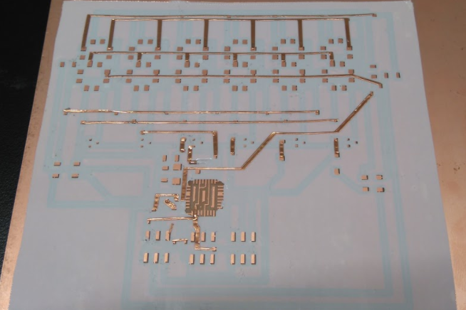
COPPER VINYL LAYER.
COPPER VINYL LAYER inverse
EPOXY VINYL LAYER.

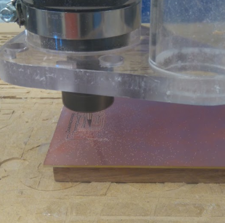
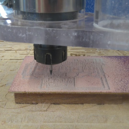
Firsty I milled the bottom layer - the tool diameter of the 1/64" mill was to larger to fit through some of the separations between traces particularly around the atmega138P and so I decreased the tool diameter in the fabmodules from 0.39mm to 0.27mm and it seemed to fit into most of the gaps.
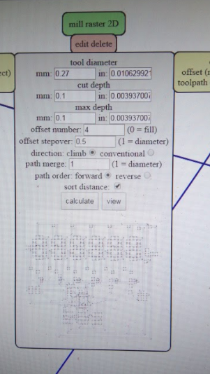
I used the shopbot to mill the board - there were no problems.
The vinyl cutting was not as streamlined. The copper traces were much too thin and therefore when the blade was cutting the copper it pulled up the traces as well. I managed to solve this by:
1) Doubling the width of the traces manually in GIMP.
2) Decreasing the force of the blade to 45g.
The epoxy on the other hand worked very well with the default settings.
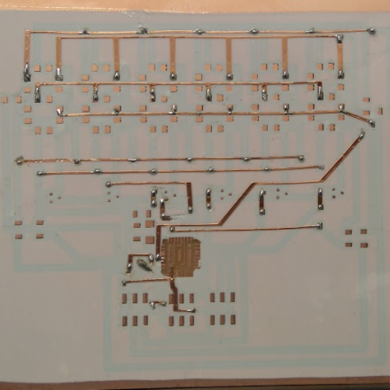
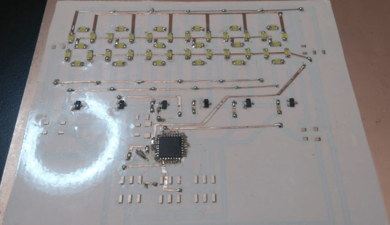
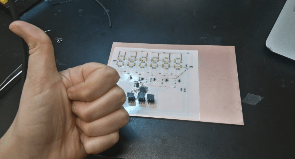
Assembling the layers took a lot of patience and time - but it all came together eventually.
Soldering also took a lot of patience and time - TIP use the Voltmeter/Ammeter/Ohmmeter frequently to make sure that there are no short circuits.
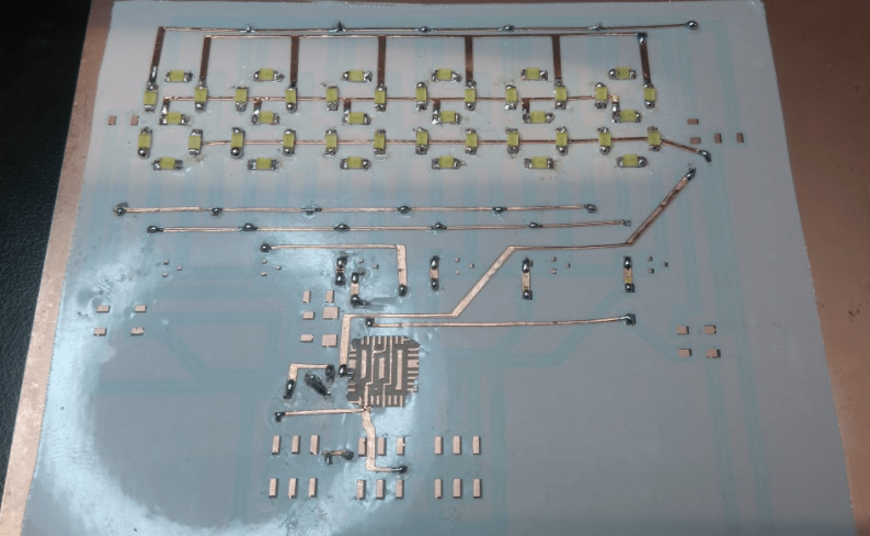
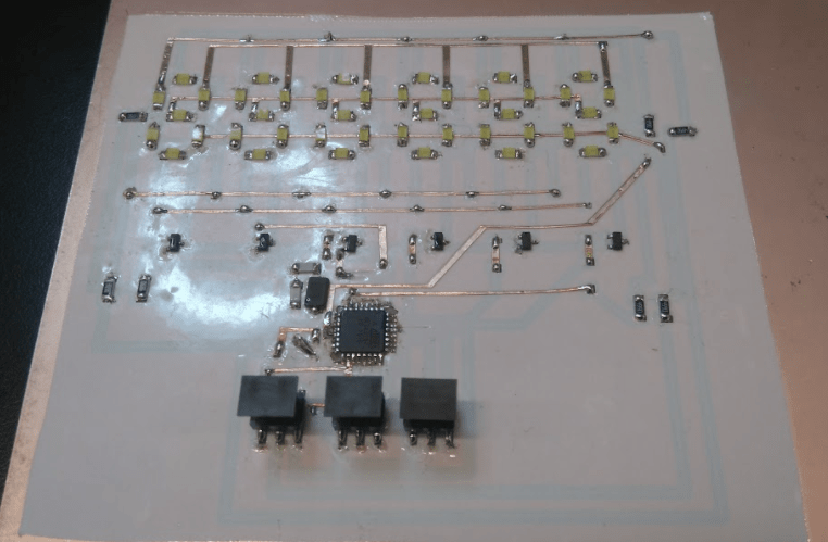
ALL DONE!.
.