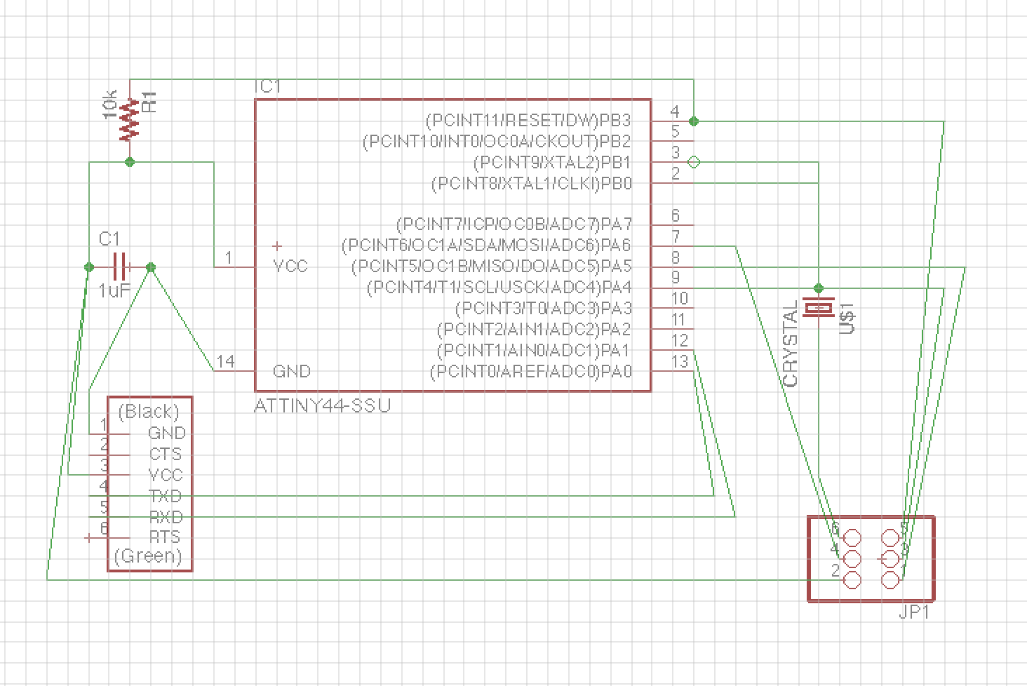
After listening to Jonah talk about how much we’re all going to hate Eagle, it was surprisingly okay to use. That is, until I got to the mysterious part labelled “JP1” which seemed to correspond to “J1 ISP” in Neil’s diagram, but instead of being labelled with the same labels as Neil’s diagram, the eagle part just had numbers 1-6. Time to Google things…
Fortunately for me, this class is incredibly well documented, and someone from fab academy had a nice diagram that informed me that 1 was in fact MISO. The rest of the initial setup went smoothly… until I ended up with a tangled mess of nets. I did my best to straight them out by moving and rotating various objects, but I still wasn’t happy.
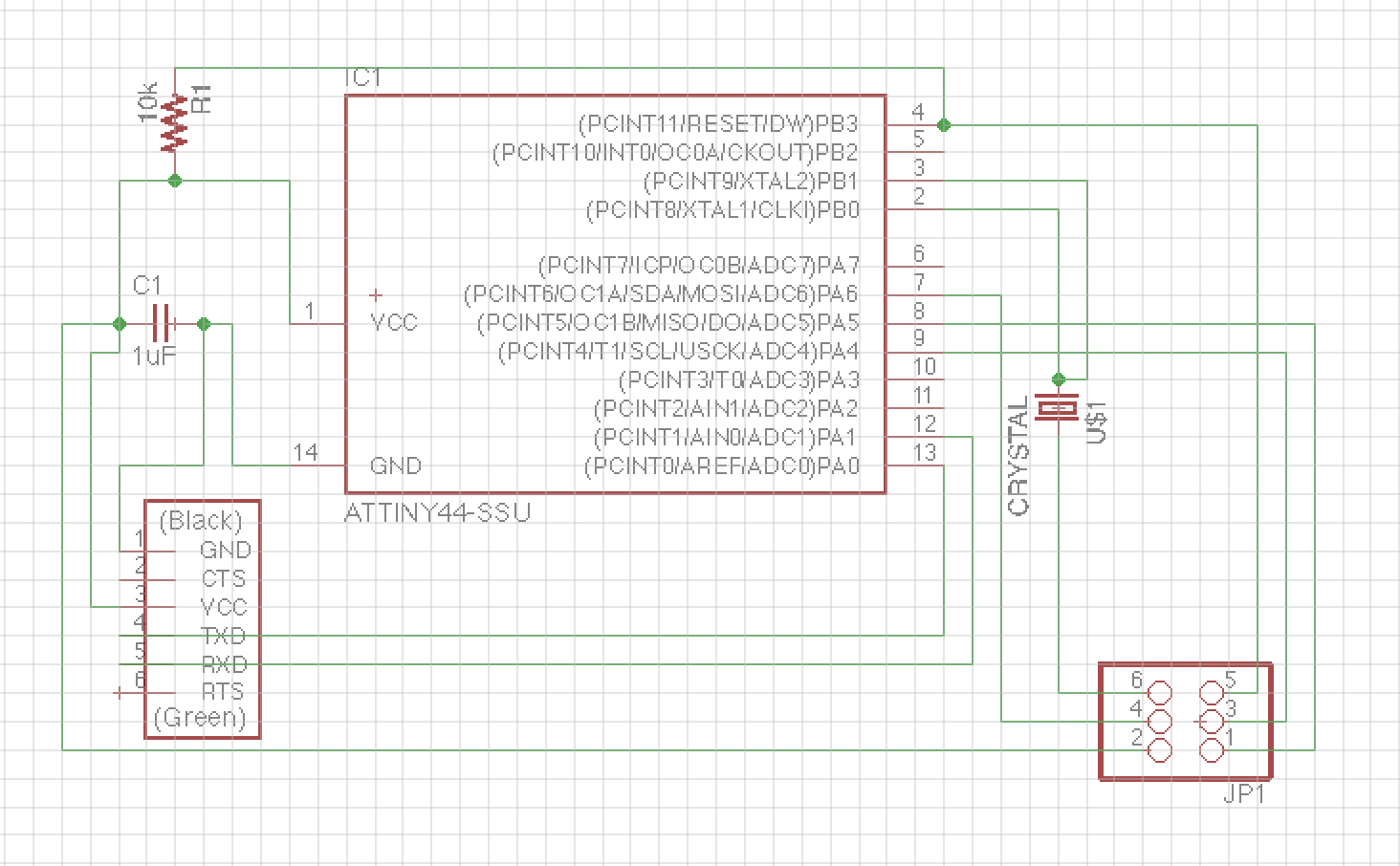
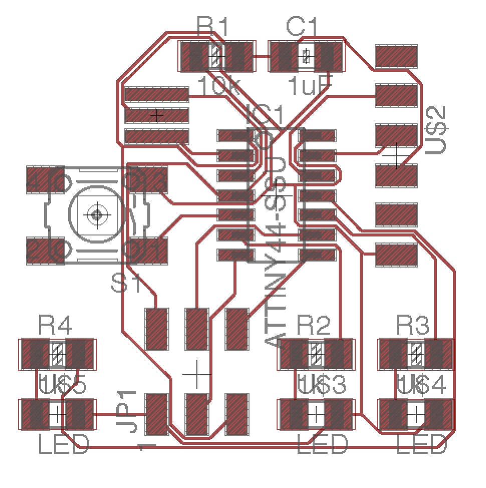
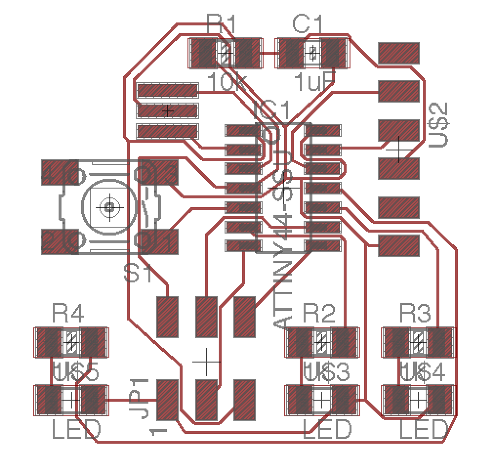
After a bit more googling, I learned that nets in come in a variety of styles, and the one I really wanted was “wire bend style 4”, which would stick to nice clean right angles.
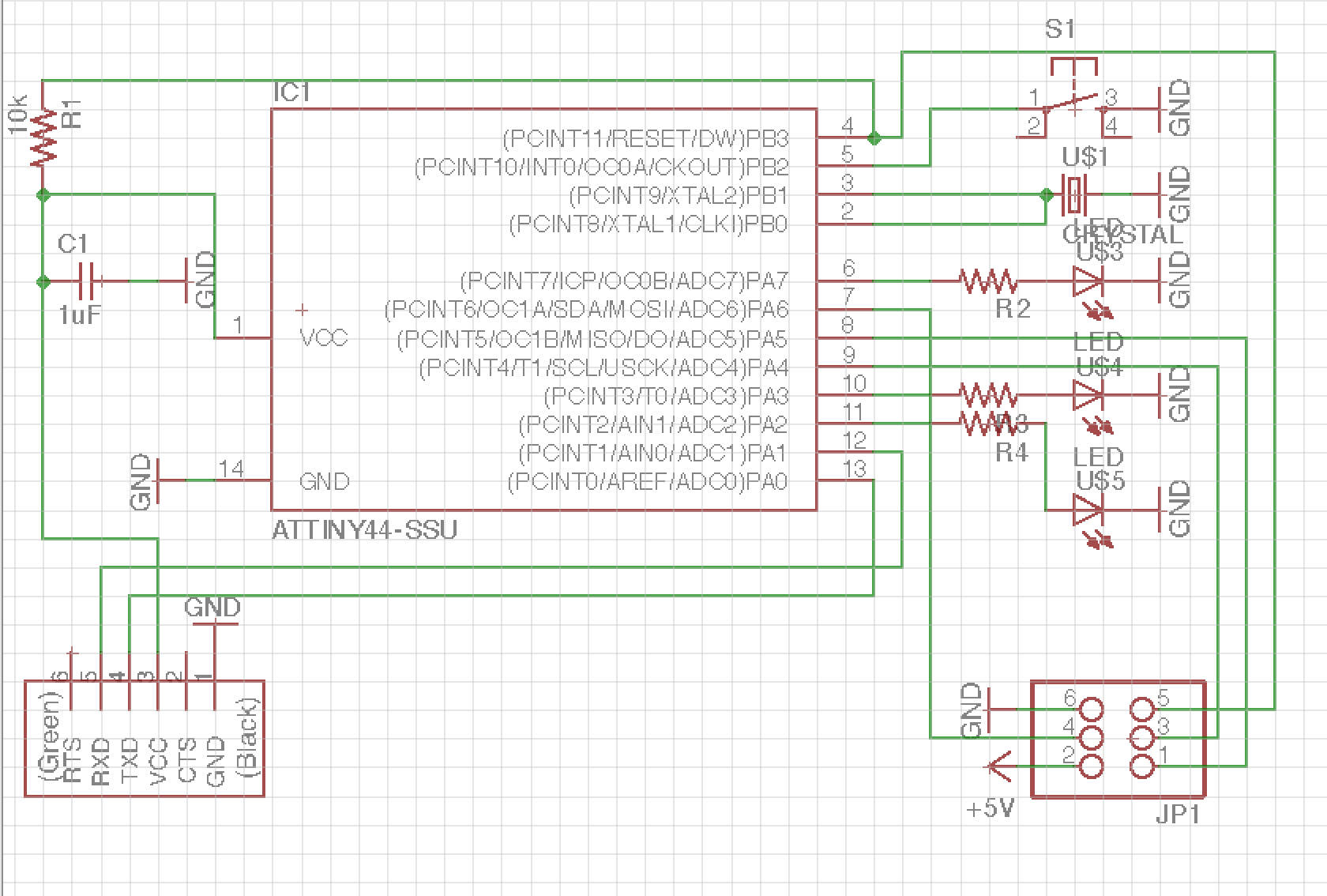
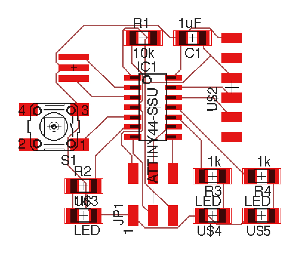
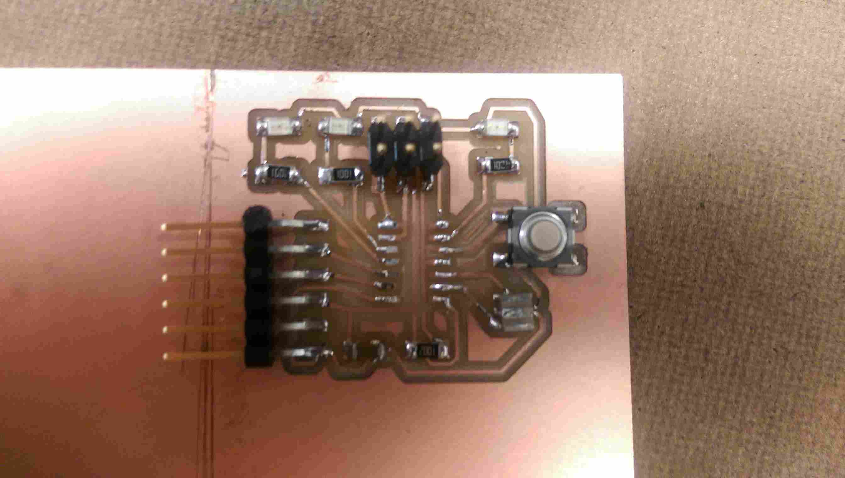
I decided to make use of all my spare pins and add three LEDs instead of just one, so I drew those in with resistors and added my switch. Then I generated a board from the schematic.
Jonah claimed that you needed to drag parts one by one onto the board, but in fact there was a quick way to drag them all by grouping and the ctrl+right click to drag the group (thanks Google!).
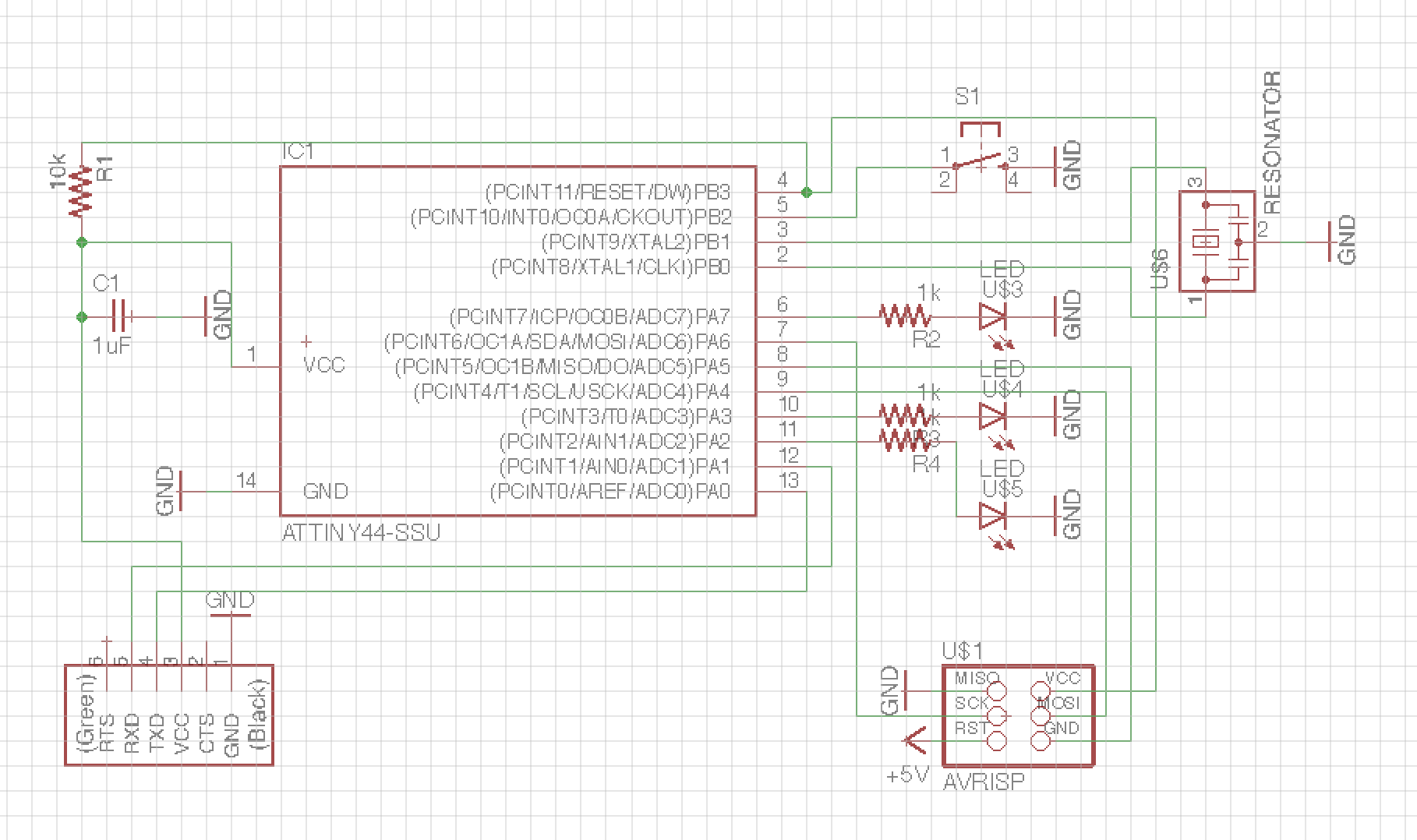
And of course, as I struggled to place the traces and had to consult previous examples, I noticed that my components looked a bit off. Sure enough, I had used a crystal instead of a resonator (an honest mistake I think considering that Neil’s diagram said “XTAL”).
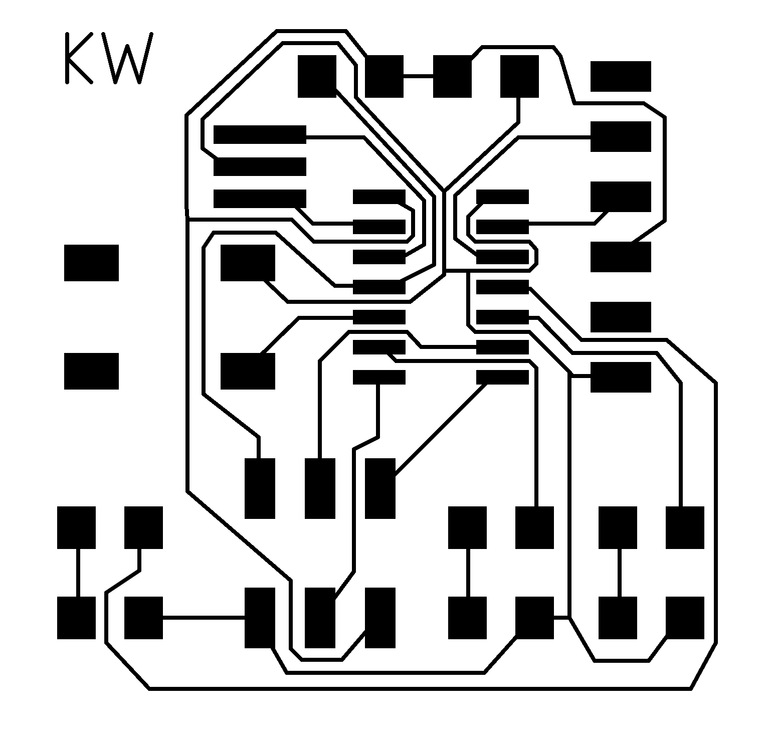
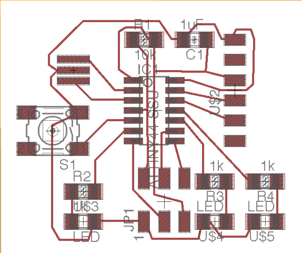
I then alternated between running the auto-router and moving things around until I no longer had vias. The traces looked a bit tight, so I moved them by hand until they were nicely spaced. Then I thickened them up to work on the vinyl cutter, exported my file, and went to bed.
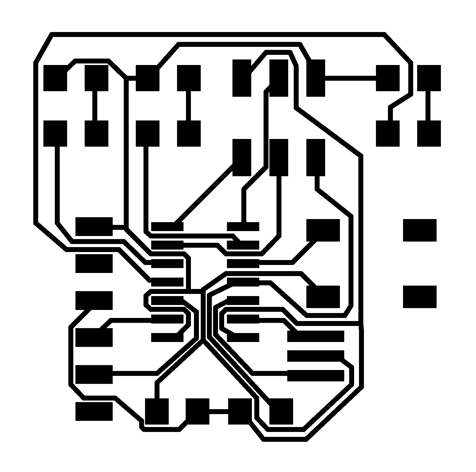
The next morning when I went to cut, there was no copper to be found. After a bit of searching, Jonah informed me that someone had borrowed the roll, and it turned out to be the only roll. I posted an issue to gitlab and waited for a response. After a day without a response, I decided to redo my board to be mill-friendly, which I thought was just a matter of making thinner traces but turned out to be a matter of redo-ing all of the traces until they no longer went between the pins of the Attiny, a process that was simultaneously really painful and kind of fun (am I secretly a masochist?).
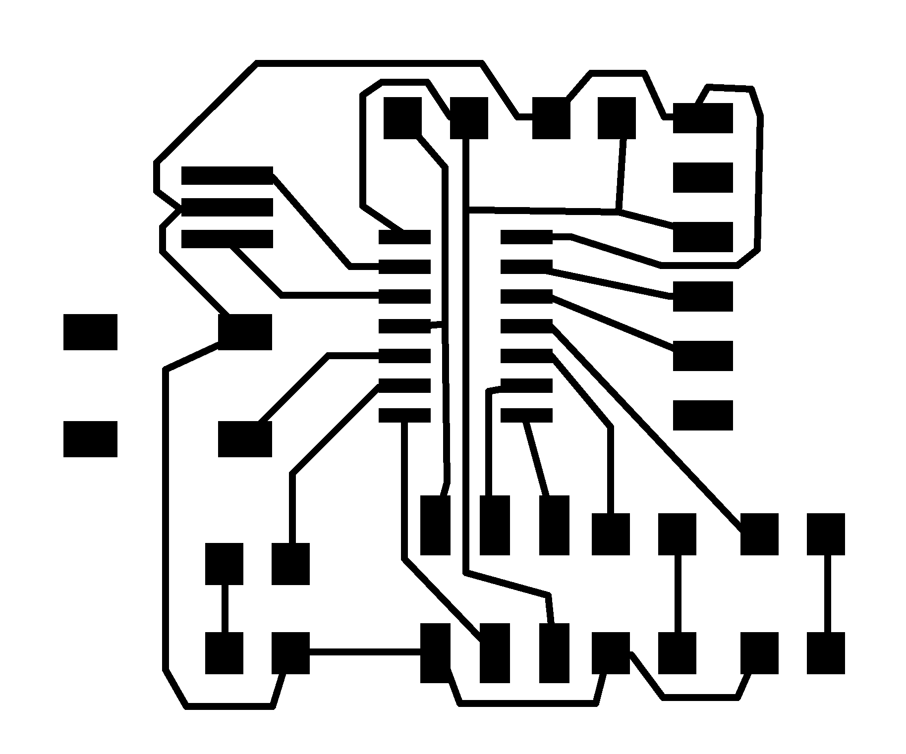
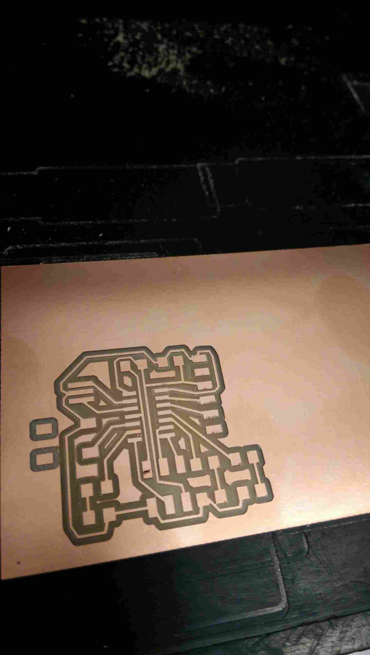
After a relatively uneventful trace-milling process (yay!), I tried to mill the outline. I figured I could just draw an appropriately-sized rectangle in Illustrator, but mods failed to read it. After a lot of tweaking, I gave up. Only days and lots of soldering later did I realize that the outline should be just a white solid shape on a black background, not a literal line. Oops. Won’t forget that next time!
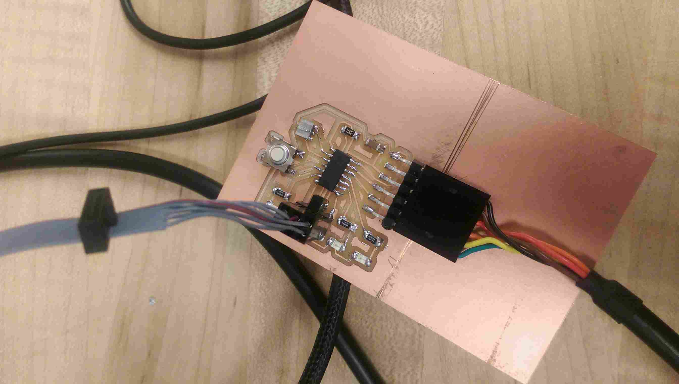
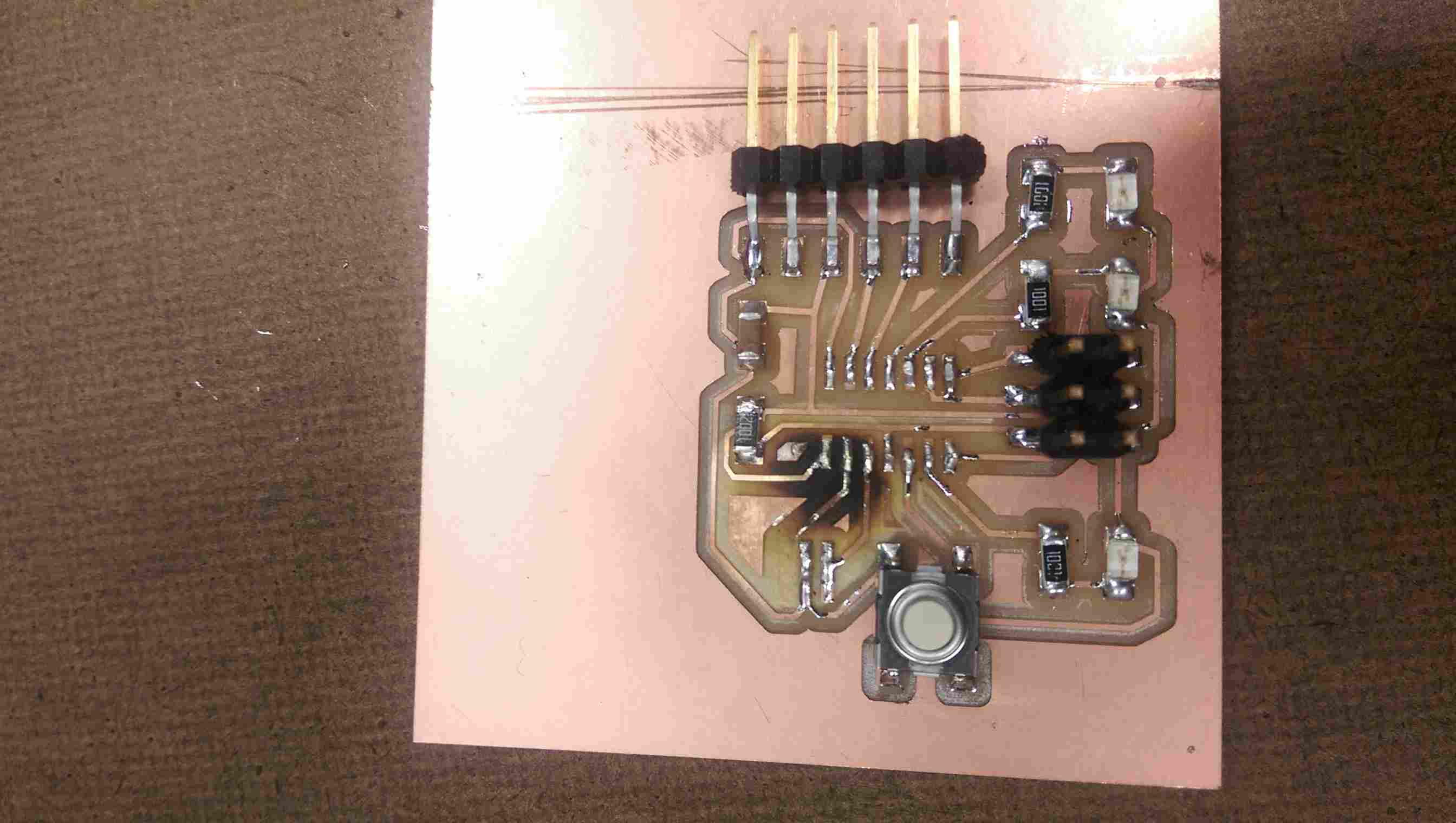
The soldering itself went relatively smoothly (pun unintended), except of course for the crystal, which would prove to (probably) be my downfall later on. It was at this point that I got cocky and assumed that I could photography the finished board later, once I had programmed it, so I didn’t bother taking a picture.
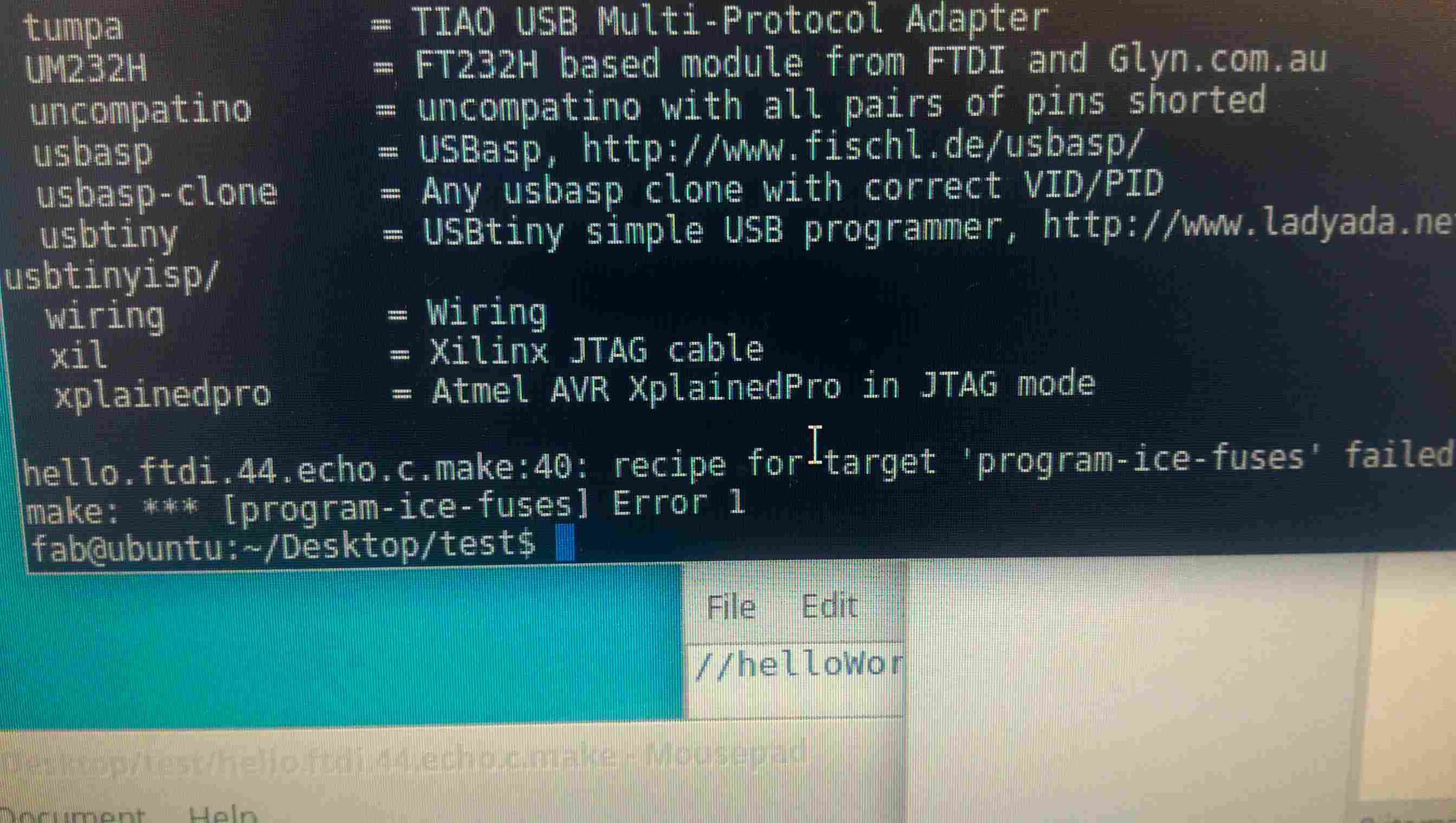
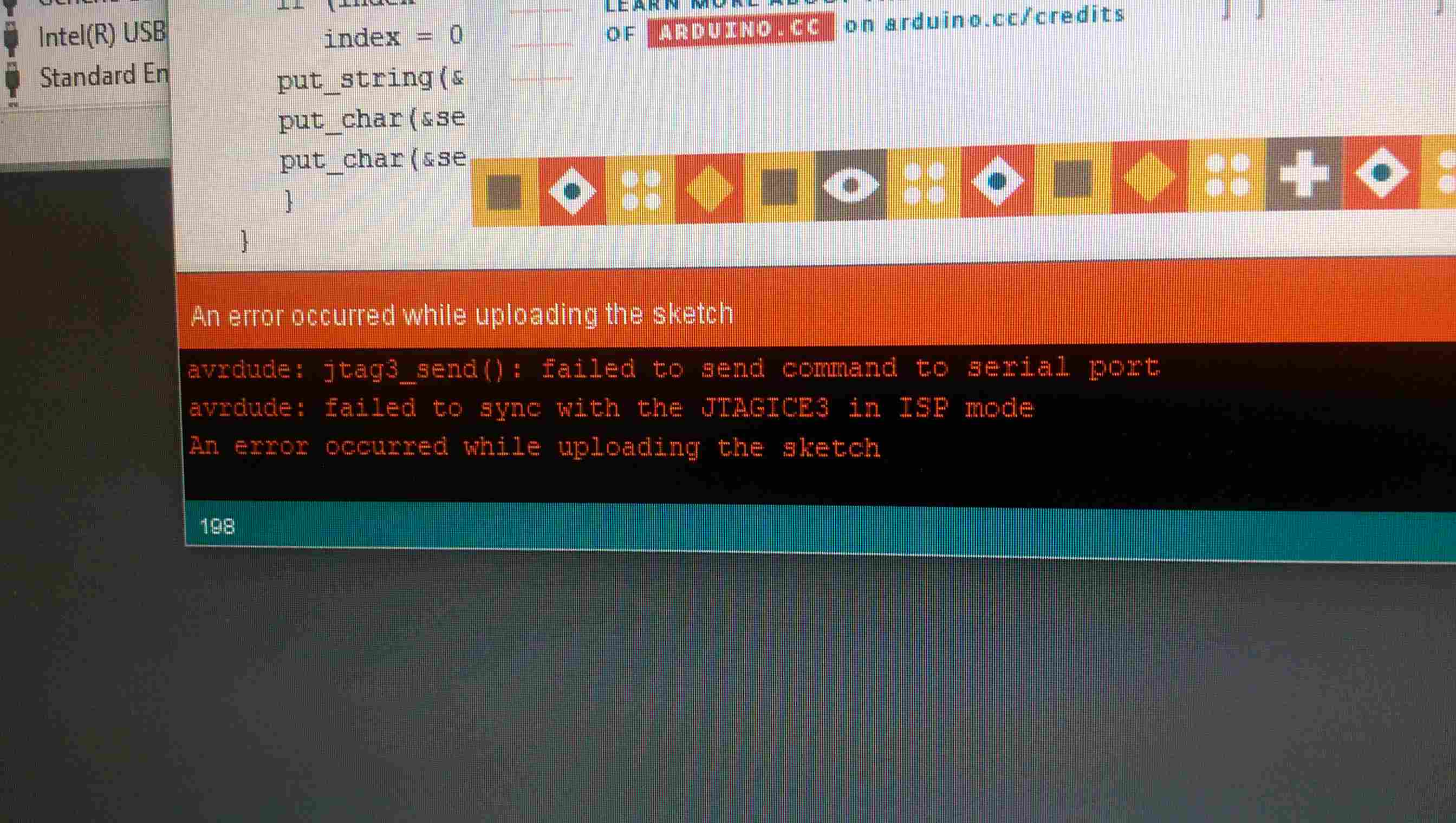
I then tried to program it, a process that involved troubleshooting remotely with Calvin and in person with Eghbal and Jonah, all without success. Things I tried: switching computers, switching operating systems, trying to use a hack that involved programming it from the Arduino interface (which we got to work on Eghbal’s board but not mine), switching programmers from the Atmel Ice to the usbtiny and back again, checking for errors in Eagle, visually inspecting the solder, reorienting all of the cords multiple times, replacing the Attiny, removing the crystal, and finally realizing that some solder got a little too flow-y and had unintentionally connected two traces in the process of replacing the Attiny. This was of course by once again heating up the Attiny to remove it, a process which produced this really fun bulge.
At this point, I had no time left to repeat the entire process and make a new board, so I decided to write this one off as a valuable learning experience. The copper did finally turn up though, so perhaps next week I’ll make a vinyl cut board.
Fortunately for me, this class is incredibly well documented, and someone from fab academy had a nice diagram that informed me that 1 was in fact MISO. The rest of the initial setup went smoothly… until I ended up with a tangled mess of nets. I did my best to straight them out by moving and rotating various objects, but I still wasn’t happy.
After a bit more googling, I learned that nets in come in a variety of styles, and the one I really wanted was “wire bend style 4”, which would stick to nice clean right angles.
I decided to make use of all my spare pins and add three LEDs instead of just one, so I drew those in with resistors and added my switch. Then I generated a board from the schematic.
Jonah claimed that you needed to drag parts one by one onto the board, but in fact there was a quick way to drag them all by grouping and the ctrl+right click to drag the group (thanks Google!).
And of course, as I struggled to place the traces and had to consult previous examples, I noticed that my components looked a bit off. Sure enough, I had used a crystal instead of a resonator (an honest mistake I think considering that Neil’s diagram said “XTAL”).
I then alternated between running the auto-router and moving things around until I no longer had vias. The traces looked a bit tight, so I moved them by hand until they were nicely spaced. Then I thickened them up to work on the vinyl cutter, exported my file, and went to bed.
The next morning when I went to cut, there was no copper to be found. After a bit of searching, Jonah informed me that someone had borrowed the roll, and it turned out to be the only roll. I posted an issue to gitlab and waited for a response. After a day without a response, I decided to redo my board to be mill-friendly, which I thought was just a matter of making thinner traces but turned out to be a matter of redo-ing all of the traces until they no longer went between the pins of the Attiny, a process that was simultaneously really painful and kind of fun (am I secretly a masochist?).
After a relatively uneventful trace-milling process (yay!), I tried to mill the outline. I figured I could just draw an appropriately-sized rectangle in Illustrator, but mods failed to read it. After a lot of tweaking, I gave up. Only days and lots of soldering later did I realize that the outline should be just a white solid shape on a black background, not a literal line. Oops. Won’t forget that next time!
The soldering itself went relatively smoothly (pun unintended), except of course for the crystal, which would prove to (probably) be my downfall later on. It was at this point that I got cocky and assumed that I could photography the finished board later, once I had programmed it, so I didn’t bother taking a picture.
I then tried to program it, a process that involved troubleshooting remotely with Calvin and in person with Eghbal and Jonah, all without success. Things I tried: switching computers, switching operating systems, trying to use a hack that involved programming it from the Arduino interface (which we got to work on Eghbal’s board but not mine), switching programmers from the Atmel Ice to the usbtiny and back again, checking for errors in Eagle, visually inspecting the solder, reorienting all of the cords multiple times, replacing the Attiny, removing the crystal, and finally realizing that some solder got a little too flow-y and had unintentionally connected two traces in the process of replacing the Attiny. This was of course by once again heating up the Attiny to remove it, a process which produced this really fun bulge.
At this point, I had no time left to repeat the entire process and make a new board, so I decided to write this one off as a valuable learning experience. The copper did finally turn up though, so perhaps next week I’ll make a vinyl cut board.