Sean Hickey
Lifelong Kindergartener at the MIT Media Lab.
Interested in learning, civic/community engagement, and pizza.
6 - Large Format Machining
FabGiantISP
This was a big week. I mean this in every sense of the word. Not only was our assignment to “make something big”, but I (perhaps unwisely) chose a project that was big in and of itself.
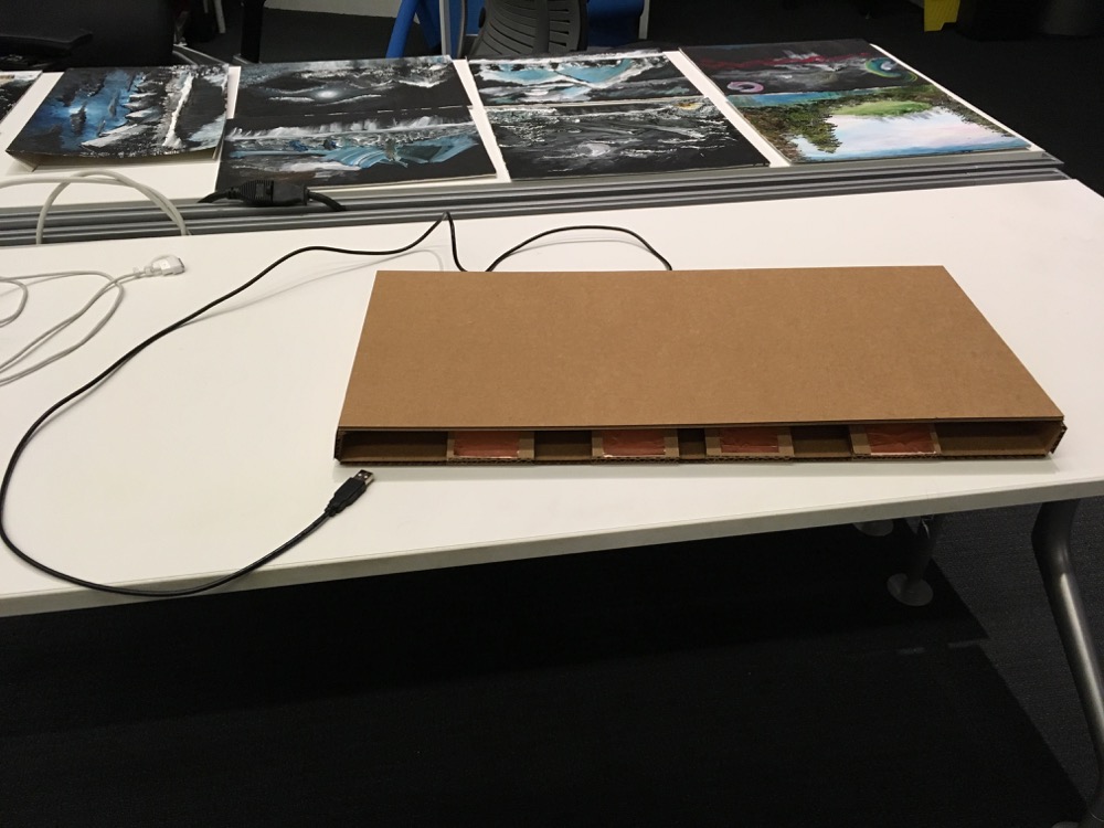
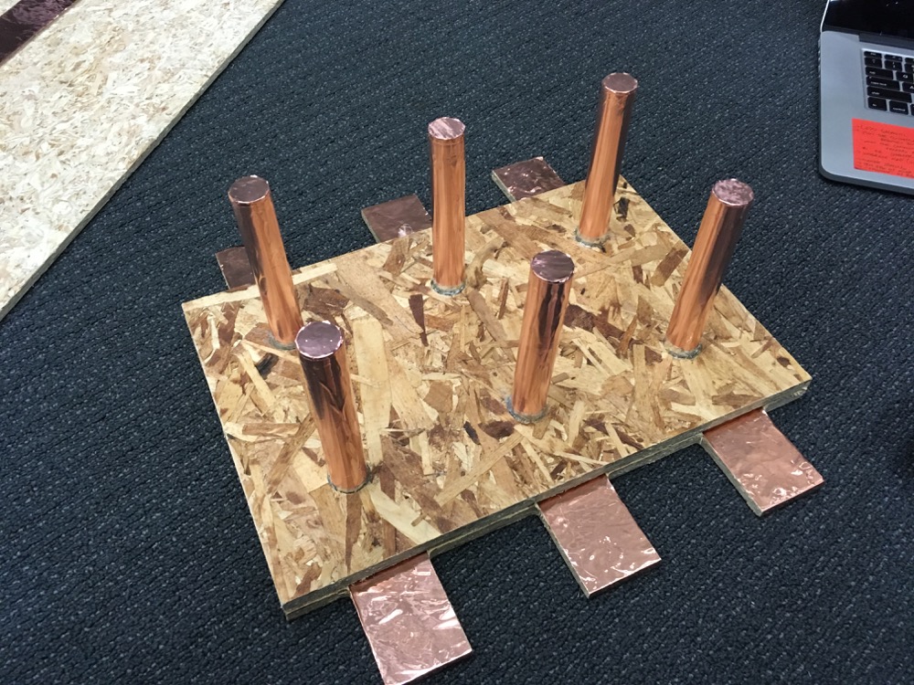
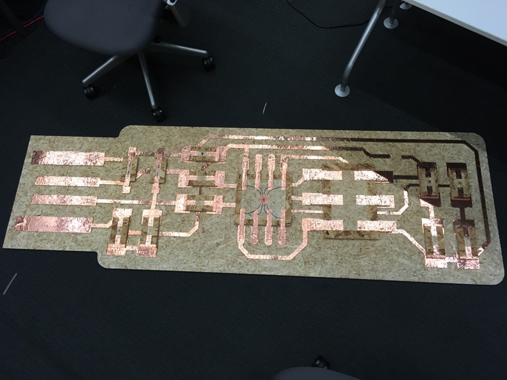
I think we can all agree that tiny things turned into giant things are funny. So for this week’s assignment, I decided to turn the FabTinyISP into the FabGiantISP. The goal was to make a fully functioning circuit board that looks just like the FabTinyISP, only 46 ⅔ times larger.
Designing the Board
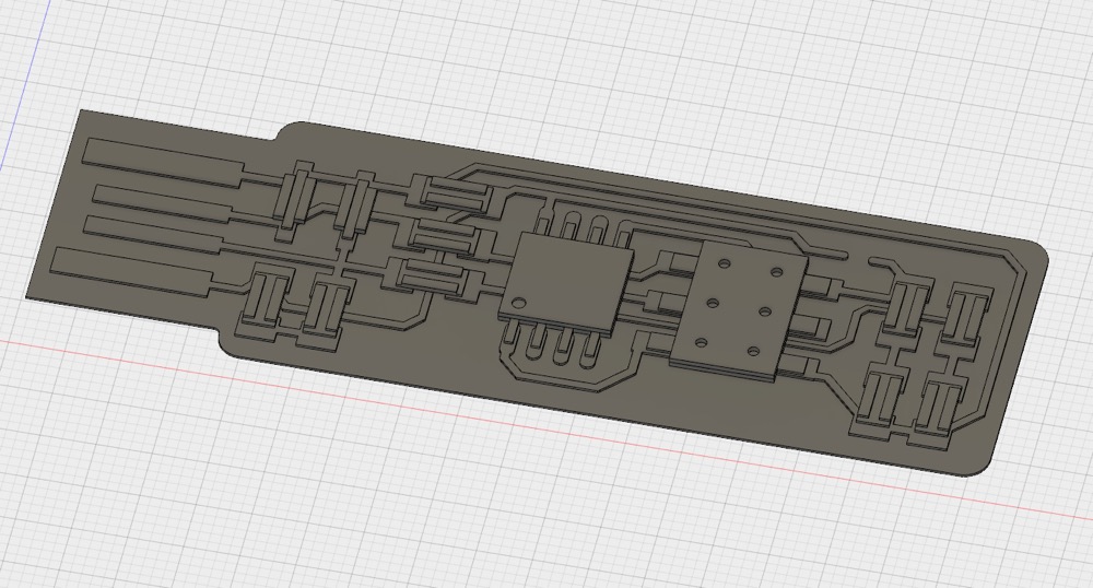
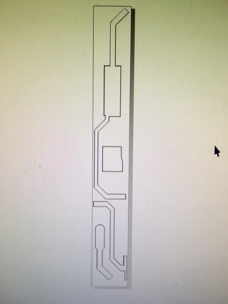
The first step was to get the vectors of the board traces and outline so that I could scale them up. Luckily, I had previously converted the FabTinyISP project into a KiCad project, so this was effectively as simple as exporting the paths as an SVG from KiCad. I cleaned these up a bit in Illustrator and then imported them into Fusion.

After laying out a 4’ x 8’ rectangle, I scaled up the vectors to a size that seemed as big as possible while still fitting comfortably on the sheet (and with room to spare to cut other components). This gave me the scale ratio of 46 ⅔.
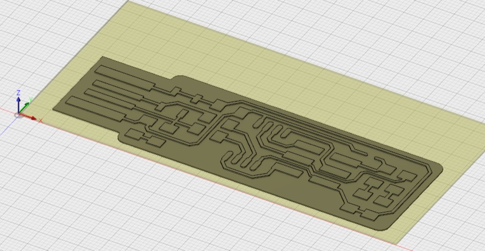
I spent some time playing around with the CAM toolpath generation tools in Fusion, just to see what it offered. It took me a little while to figure out how to get the right type of pocket toolpath given the modeled object, but in the end got something that looked reasonable.

One thing that I noticed after scaling up the traces was that there were a number of weird bumpy artifacts at several of the corners, which were probably indistinguishable when the board was tiny, but very clear on a giant model. I cleaned these up directly in Fusion leaving a nice model behind.

Designing the Components
I decided that if I’m going to do this project, I’m going to do it right and actually make the circuit work with all components in the correct physical locations. This meant figuring out how to model the components in such a way that they would easily attach to the board and look similar to the original package, but also have space to embed the actual functional component inside. After getting dimensions for the 1206, SOD123, IC, and header packages, I scaled up them up and pocketed out space in each to embed the component.
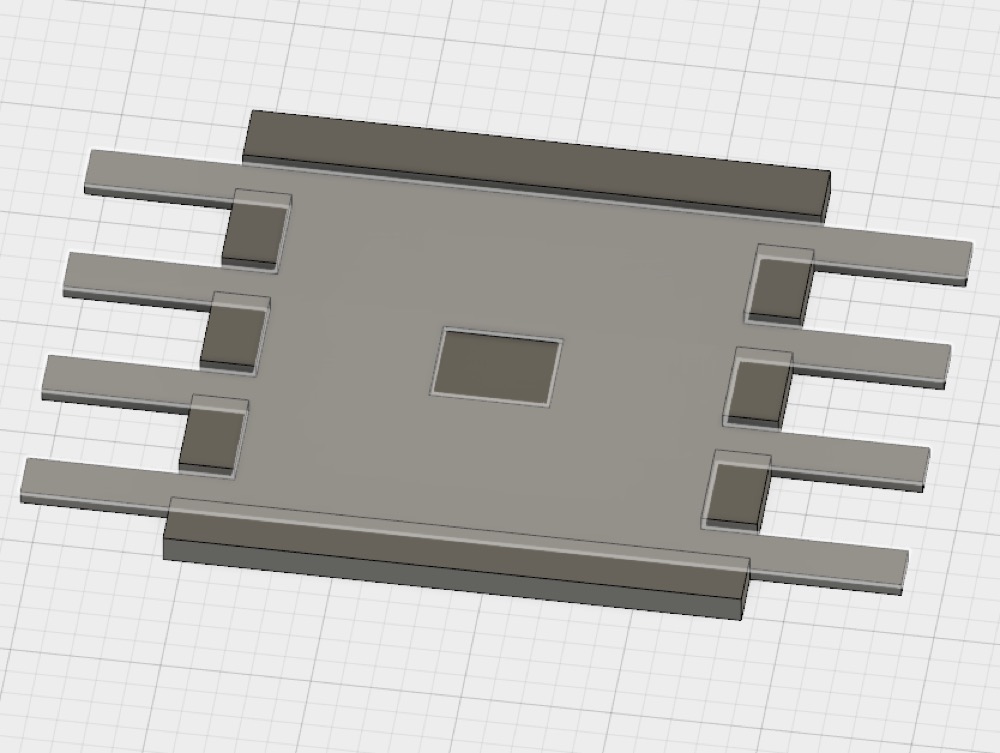
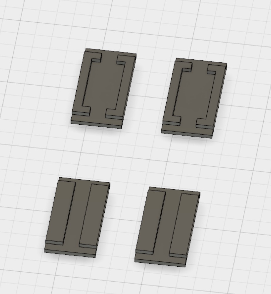
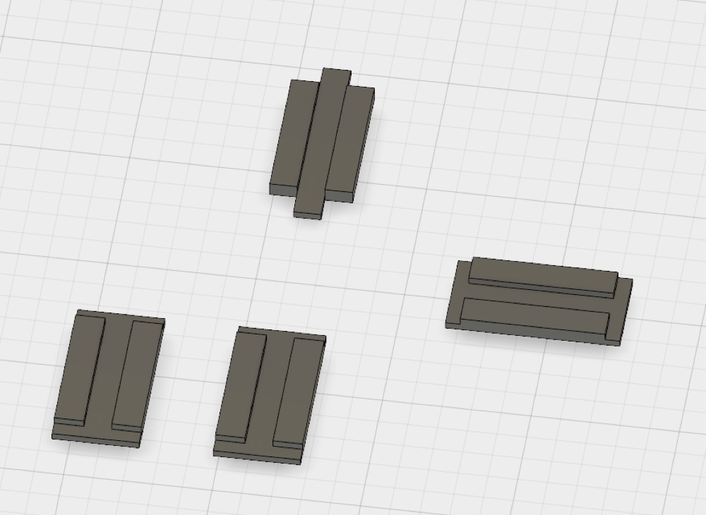
Once I had all the components modeled, I put them in place on the board to get a complete model of the board (with the exception of the header ‘pins’ since I wasn’t exactly sure what kind of material I would be able to use to make those).
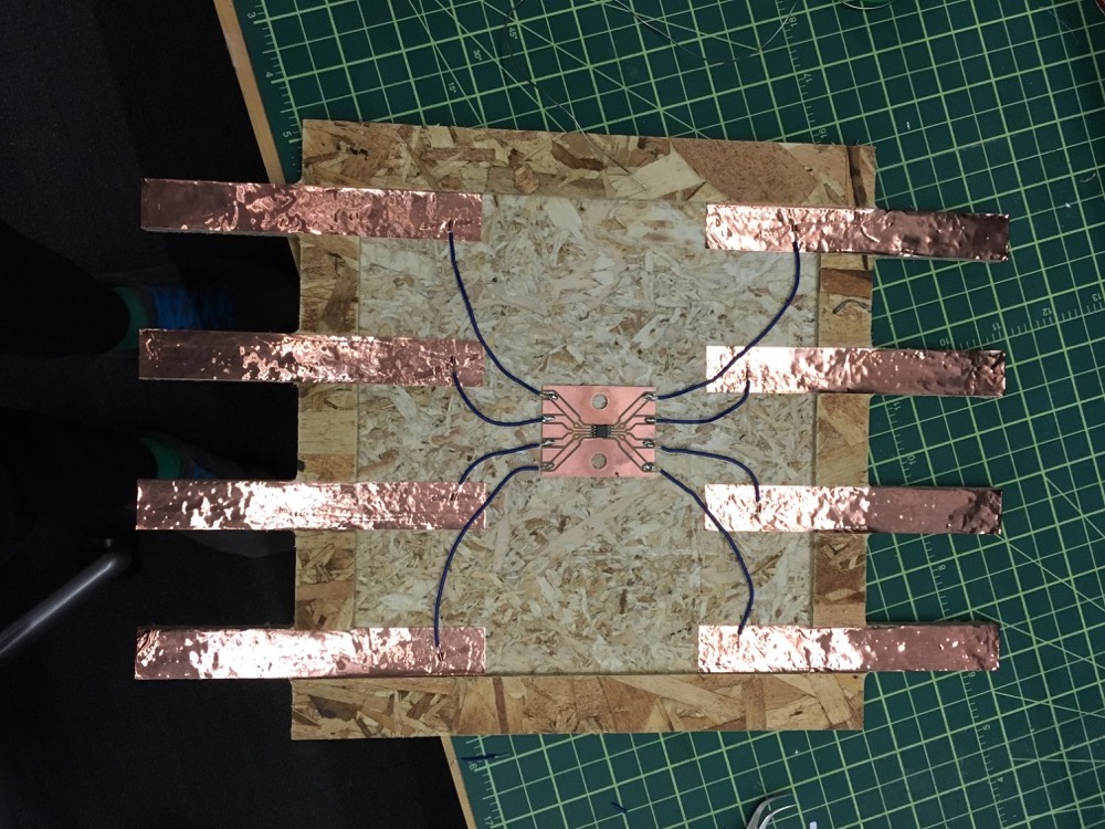
Aside 1: ATTiny45 Breakout Board
While modeling the IC component, I realized I needed a way to connect the scaled up traces to the tiny pins on the chip. I figured rather than try to somehow solder the chip pins directly to copper tape or something equally difficult, I could pretty easily make a breakout board to make the pins easier to attach to. It took just a few minutes in KiCad to put together a simple breakout layout.
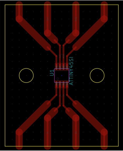
Milling was straightforward

And after soldering, I had a nice little breakout board that would be much easier to embed into the giant IC.
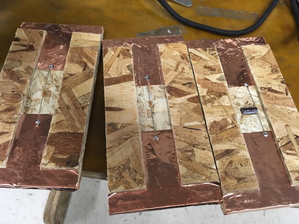
Aside 2: Through Hole Components
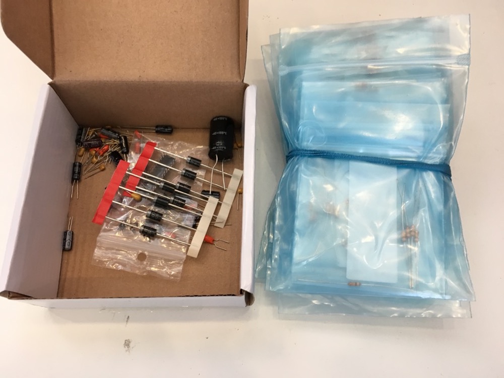
At this point, I realized that creating a breakout board for each of the rest of the components would be a huge pain. I put a call out to the class to see if anyone had any through-hole resistors, capacitors, etc. and Jake came to the rescue. Thanks, Jake!
Nesting Parts
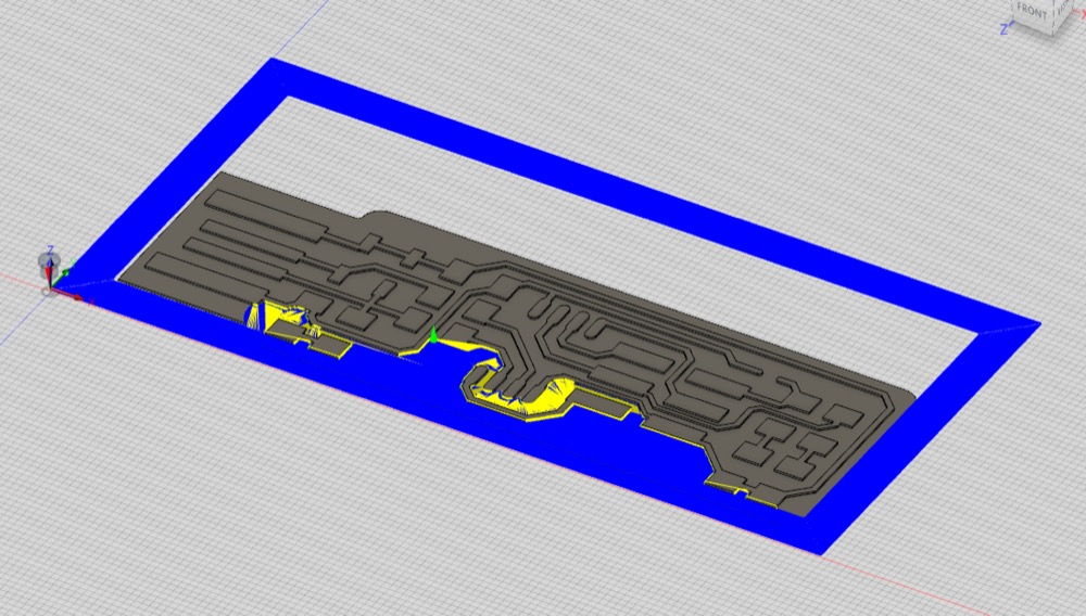
Now that I had the model complete enough to cut, I needed to nest the parts inside a 4’ x 8’ rectangle to prep for toolpath generation. This actually turned out to be quite easy in Fusion. I simply duplicated all the components, hid the originals, and repositioned the parts such that they fit in the 4’ x 8’ footprint and sat on the XY ground plane. This was nice, too, because Fusion would maintain the link between the duplicates and the originals, so if I needed to go back and change part of a component’s model, the nested layout would update automatically.
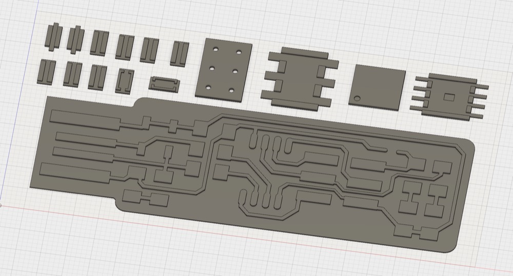
I then created a projection of all the vectors onto a 4’ x 8’ plane above the nested components and exported it as a dxf.
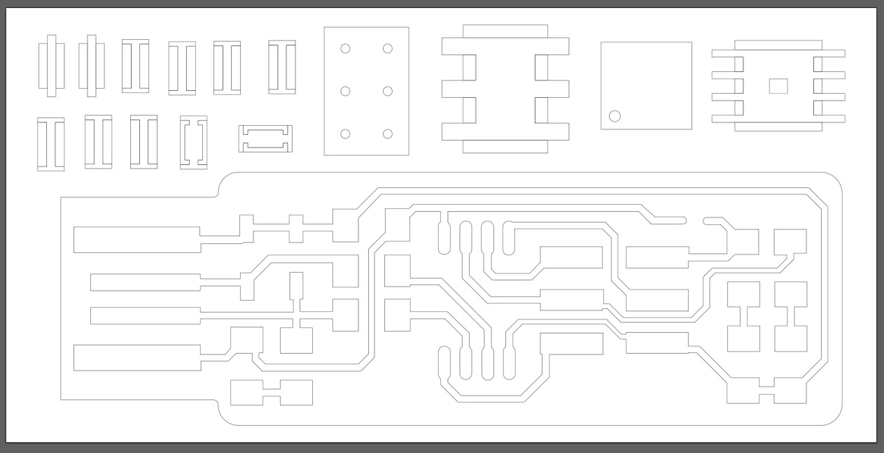
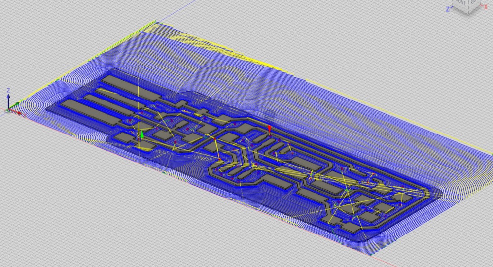
Toolpaths
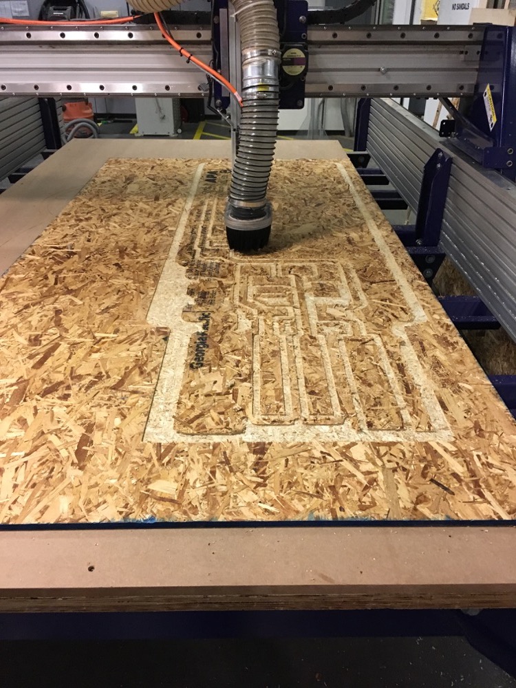
The initimable Tom Lutz was supremely helpful in getting the toolpaths generated for this project. He had a lot of good insights in terms of the complexity of the pocketing and which bits to use to make the process as easy as possible. He helped me find this monster 5/8” bit which helped bring down the total cutting time considerably.
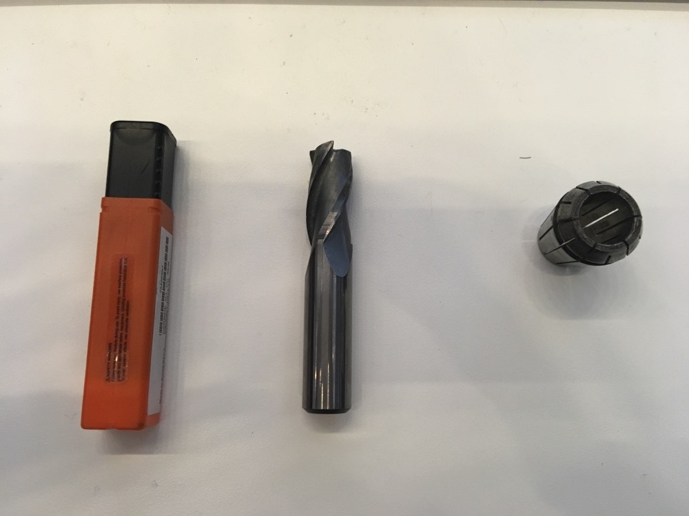
He then helped me think through the setup for a bit this size (e.g., lower RPMs since the larger diameter would mean the outside of the bit would be going considerably faster than a smaller bit) and generate the pocketing toolpath to mill the traces out.
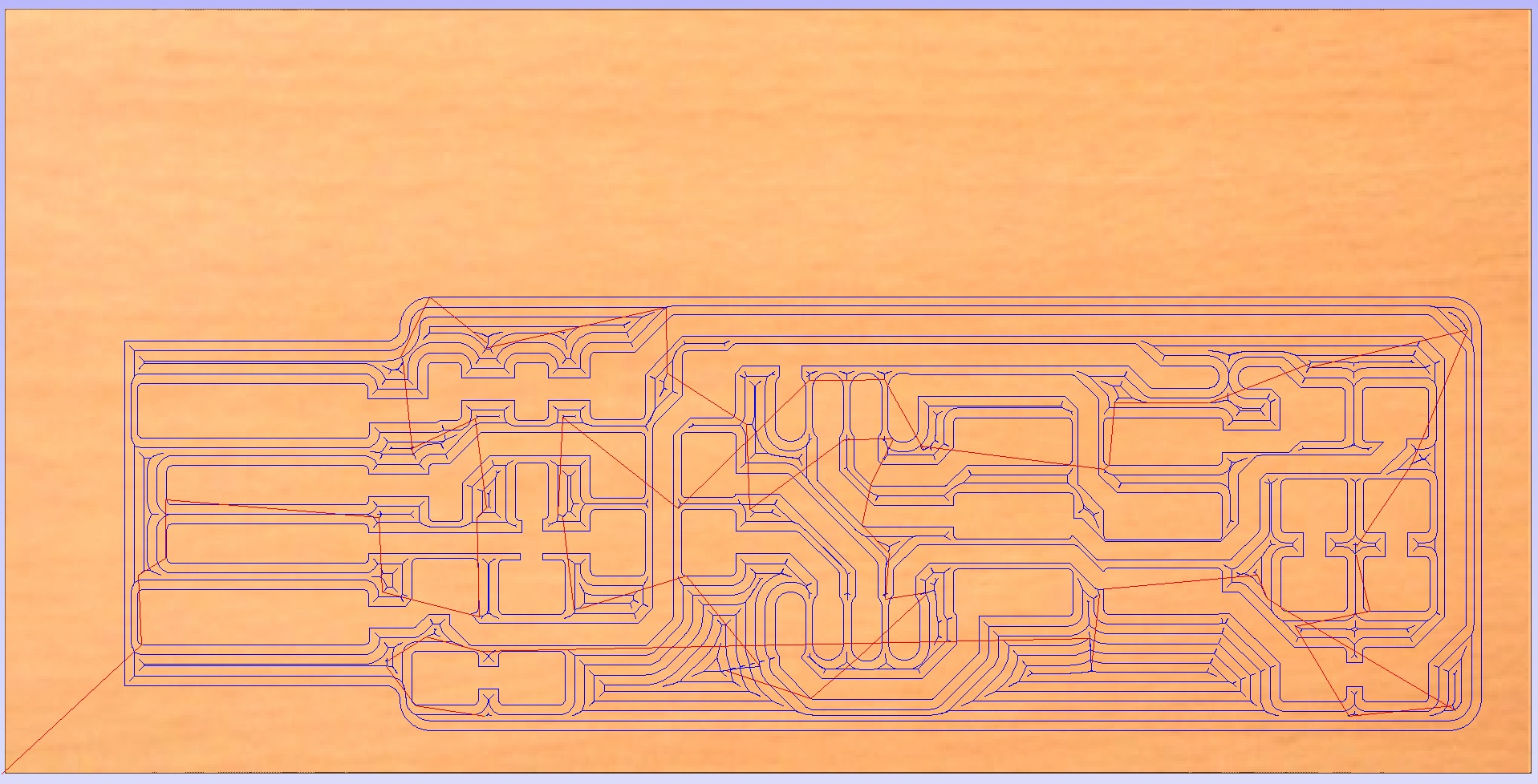
The rest of the paths were fairly straightfoward. Using a 1/4” bit, I generated the toolpaths for the pocketing on the components, drilling the holes in the ISP header, and the profiling operation to cut all the parts out of the OSB stock.
Aside 2: Giant USB Port
At some point throughout the drawing process, I realized that in order to make this thing actually work, I would need a way to plug the board into a USB slot. So, after finishing generating the toolpaths with Tom, I spent some time designing and laser cutting a cardboard USB connector of the appropriate size. I created a design with 4 rectangular extensions for each of the USB pins, and then made partial cuts evenly spaced along their length so that I could bend them into semi-spring loaded connectors.

I then put copper tape on each and cannibalized an old USB cable to expose the leads.
I soldered each respective wire to its lead, which turned out to be harder than I expected. Oddly, the soldering irons we use for electronics here were far too nice/fine to make the kind of big blobby joint I needed (more on this later).
After some hot gluing to keep the wires in place, I closed up the cardboard leaving me with a USB-A to USB-G (for Giant) cable.
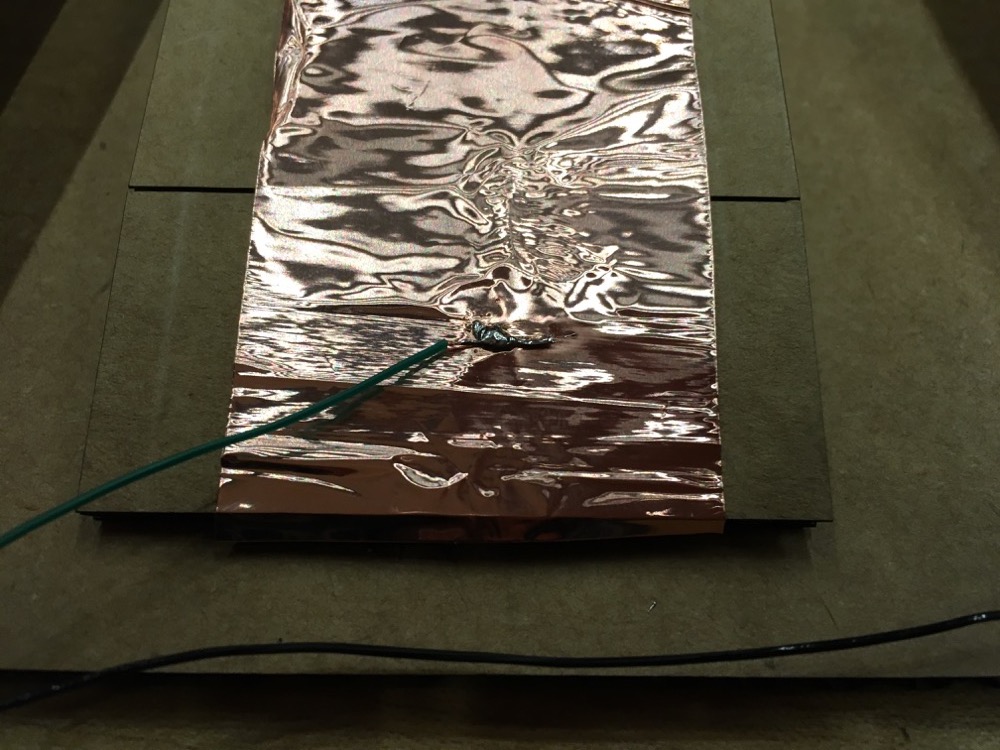
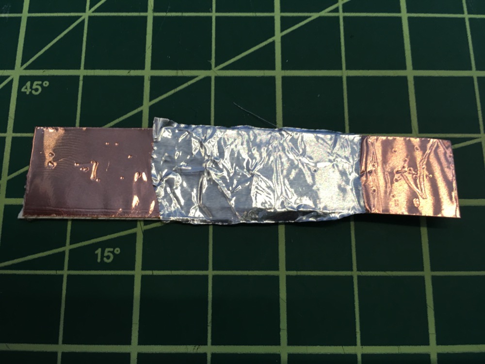
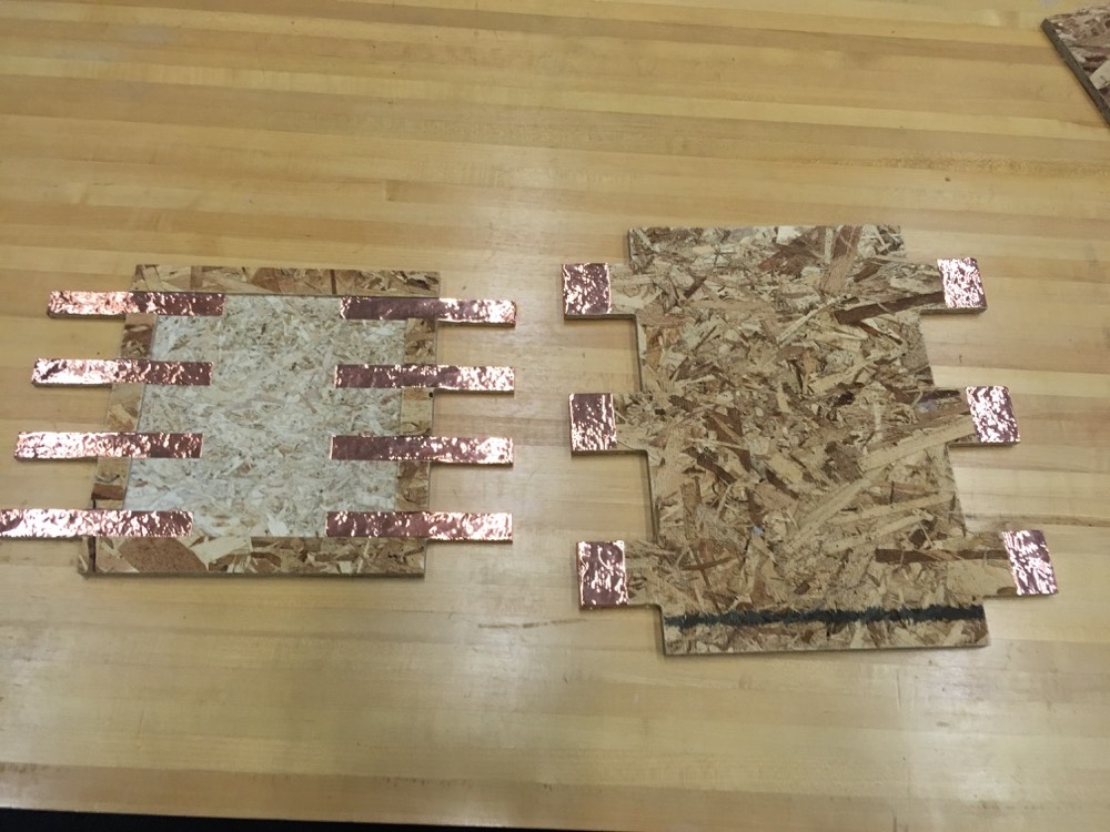
Aside 3: Copper Tape Joints
I realized that at the scale I was working, there was no way I way going to be able to vinyl cut some of the copper traces in one fell swoop. So I experimented a little with overlapping copper tape and seeing what that did to the connection. Interestingly, I found that putting a small piece of regular foil tape across the copper joint helped connectivity noticably.
Cutting
The next day, on Saturday, Tom helped me out again by aiding me in getting the ShopBot set up and making sure the giant bit wasn’t going to cause any problems. After getting everything ready, we hit go, and the traces milled like a charm.
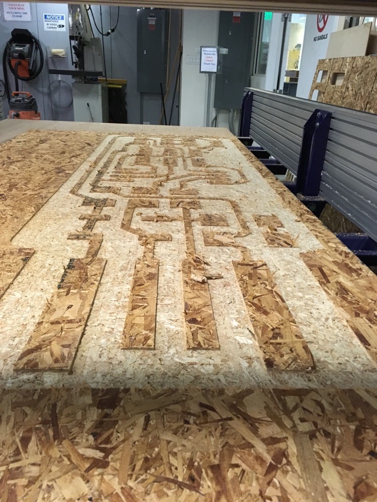
Swapping the bit out, the rest of the cutting went off without a hitch as well (splinters, aside).

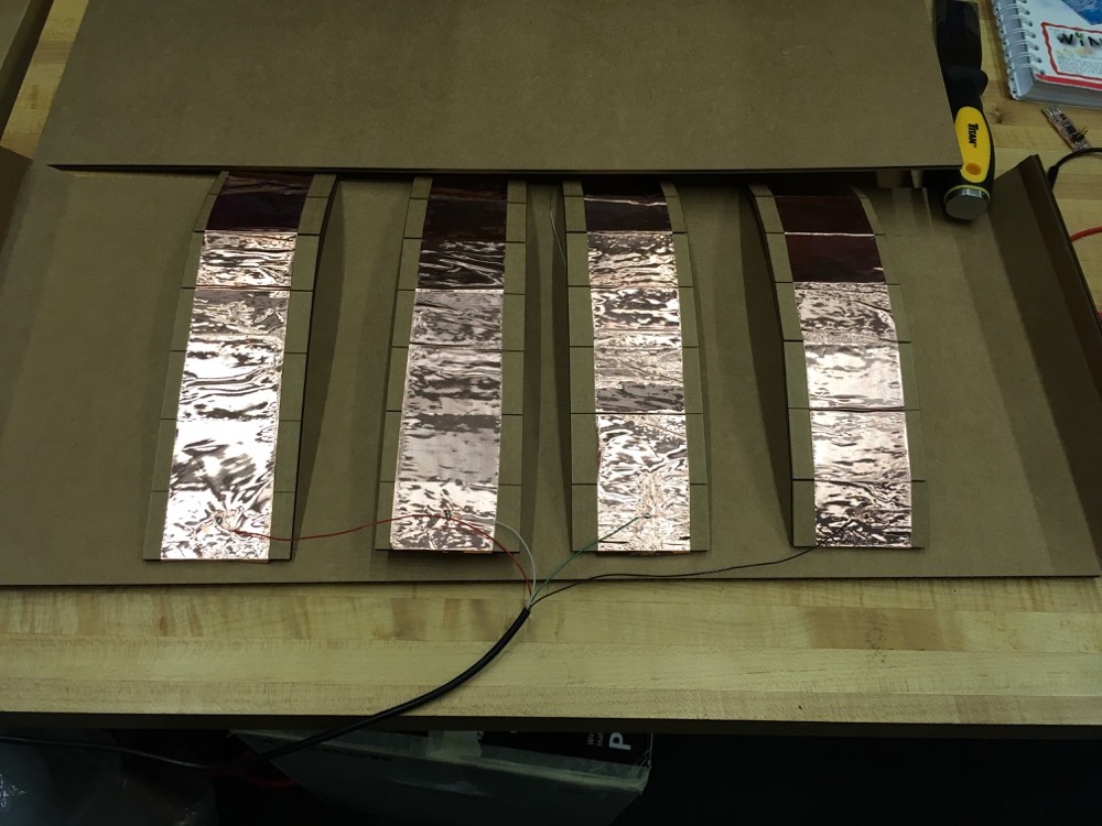
Traces
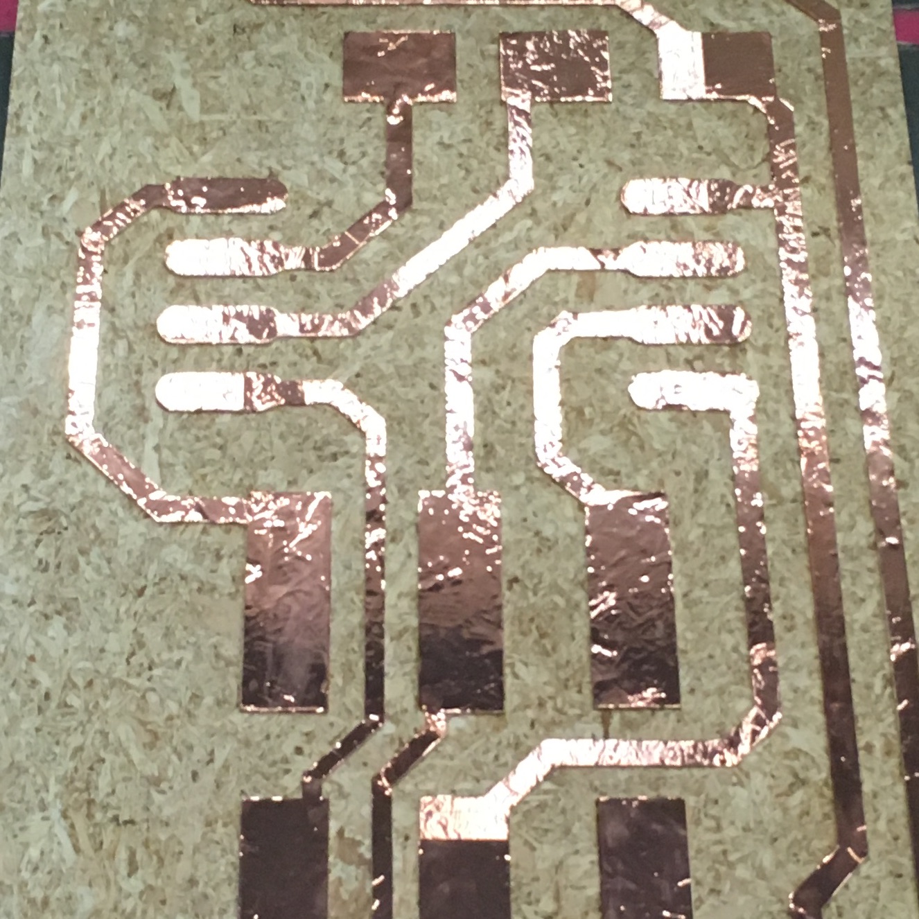
After a LOT of sanding, I started experimenting with vinyl cutting the copper foil tape and putting it on the board. This turned out to be mostly straightforward. Since the scale was so big, there was no need to use transfer paper, so I could basically just peel each trace off and place it down like a sticker.
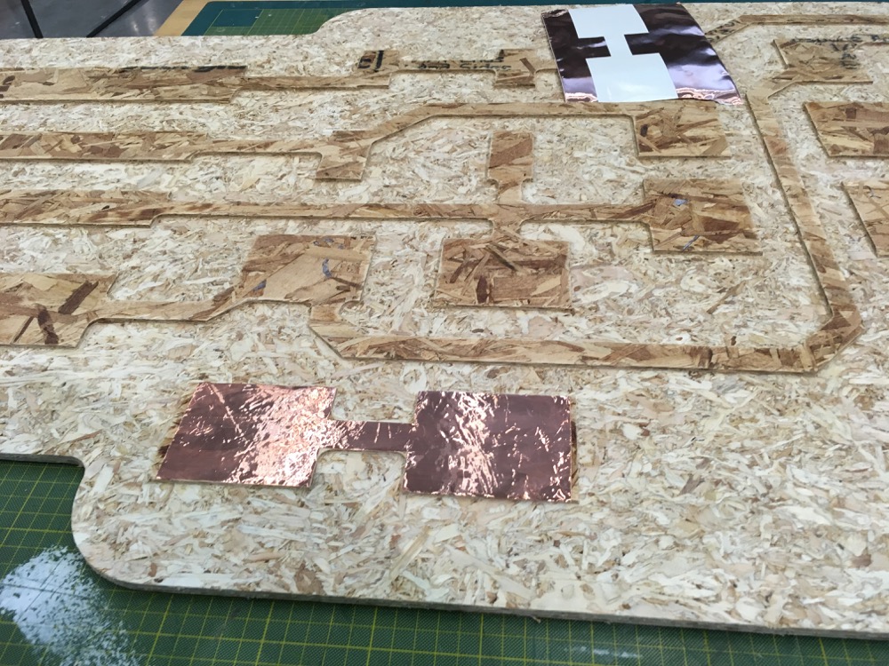
A lot of the traces were too big to fit on the 6” copper tape, so I had to cut several of them into pieces and reassemble the traces on the board.
The end result was pretty awesome (and shiny to the point where it was hard to photograph).

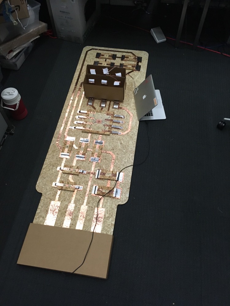
Component Assembly
After finishing the traces, I vinyl cut copper to act as leads on the various components. Each piece of copper started around the bottom of the component (so it would touch its respectively pad when placed down on the board) and then came around the top of the board so that an actual electrical component could be soldered to it.

Before leaving home that morning, I remembered that we had a 1” x 36” dowel sitting in our kitchen (left over from the previous tenants) that would be the perfect size for the ISP pins. I cut it down into six inch sections and covered each in copper tape.
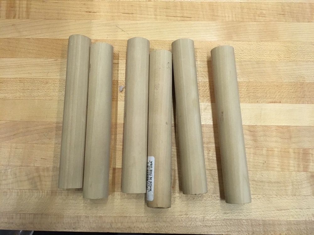

Then I taped these down to the ISP header component board, put the board with the holes on top, and hot glued the space between the dowels and the holes to keep everything snug and in place.
From there, I started to put the electrical components in place. At first, I tried just copper taping the components down, but quickly realized that wasn’t go to be reliable at all and that I would have to solder everything. Again, I got frustrated by trying to solder big things with a tiny precision tip, so I went down to the electronics shop and dug around in the bins until I unearthed a very old, beat up, blunt solder tip from who knows when.
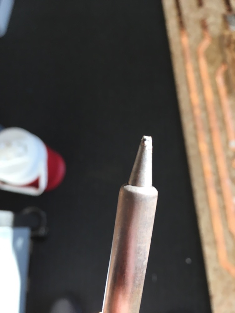
It worked like a miracle.
Once all the components were complete, I placed them on the board to get a sense of how everything would fit together.
“Soldering” the Components
In thinking through the best way to connect the components to the board, I remembered how joining overlapping copper tape with foil tape actually worked pretty well. So I used foil tape to connect the components. I espcially liked how this sort of looked like solder on the board, and I even went ahead and taped the connections down at an angle to look more like a solder joint. This worked well.

With everything “soldered” in place, the thing really started to come together.

I was very nearly ready to test my creation, except for one missing piece:
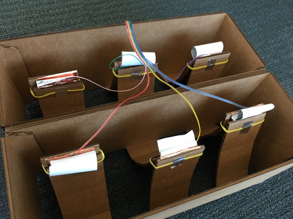
Aside 4: Giant ISP Socket
Building off the success of the giant USB port, I used the same semi-cut curved cardboard structure to build a socket for the ISP header. Each slot had two foiled cardboard curves (connected on top by foil tape) that (in theory) would touch either side of the pin as the pin was inserted. Each of these was soldered to a ISP cable with a standard sized connector on the other end.

This design kind of worked, but without gravity to assist (as in the case of the USB port), the curved pieces of cardboard didn’t always fall against the pins in the right way. Still, after jiggling it into place and testing the connectivity with a multimeter, I was ready to test.
Flashing the ATGiant
I plugged the board into the giant USB cable (or more accurately, plugged the cable around the board), hooked up the ISP header to my small ISP programmer I made a few weeks ago, and hooked them both up to my computer. Some LEDs went on! A good sign! Then, I ran make flash and…
It worked! Kind of! I think??!
So the first time I flashed the chip, it actually did successfully transfer (according to avrdude). However, I couldn’t get make fuses to run correctly and then kept running into a bunch of issues where my computer wouldn’t properly recognize the giant board, or avrdude would throw an “invalid device signature” error.
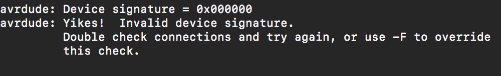
It was late and I was tired, so I went home.
Making It Look Purty
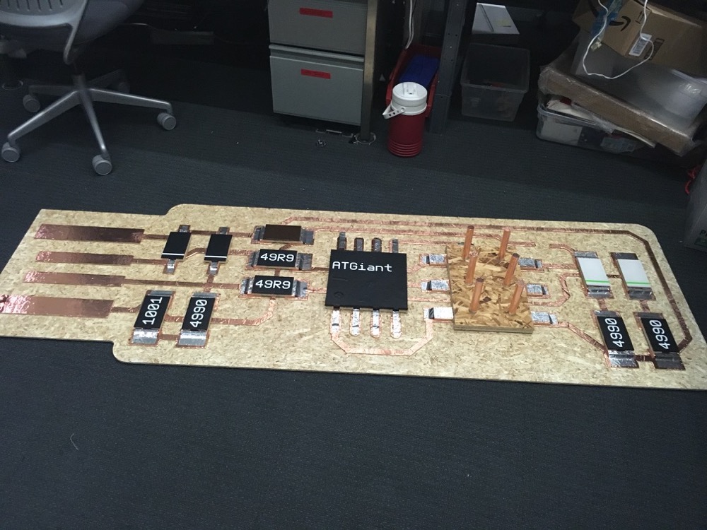
I figured if the thing wouldn’t actually work as a programmer, at least I could make it look like a nice object. So I spent some time down in the shop laser cutting cardboard tops for the components and vinyl cutting covers and part numbers to put on top.

I realized I still wanted the components to be accessible (in case I ever could get the thing to work in the future), so I simply used painter’s tape to secure the covers. At last the board was fully assembled.
Plot Twist
I had a little bit of time left on Tuesday afternoon, so I did some investigating into the weird invalid device signature error. From what I gathered, this usually occurs when there is some finicky connection. This brought me back to the ISP socket and wondering how I could make it work better. Eric Rosenbaum in LLK had a great idea of simply putting rubber bands around each pair of connectors to hold them against the pin. After putting these on, the whole socket worked better in general. Everything was more aligned and sturdy, and the leads held against the pins with no problem at all.
I plugged everything back in and lo and below, the thing programmed successfully! I checked in the Mac system report and comfirmed that it did indeed program as a USBTinyISP. (If I had had the forethought to rebuild the firmware, I suppose I could have named it USBGiantISP…oh well). I tried to run make fuses but kept getting errors about not being able to find the device. At this point, I realized that, completely ironically, it may be my original thumb-drive sized ISP programmer that has the finicky connection (ugggggg). But after a few tries, both make fuses and make rstdisbl worked leaving me with a fully functional FabGiantISP programmer.
The Final Test
Truly, the only way to know if it worked correctly was to program another board with the FabGiantISP. I grabbed my hello world board from last week, changed the code into a simple “blink” program, and ran make. A few seconds later:

And lo and behold:

Phew.
