I took MIT 6.152J which is a course on using nanofabrication tools, basically equipment that makes nano-sized features like semiconductors, cantilevers, microfluidic channels, etc.
Nanofabrication follows several steps: Wafer pre-process (below), Resist Coating/Exposure/Development (aka lithography), Etch, and Post-Etch.
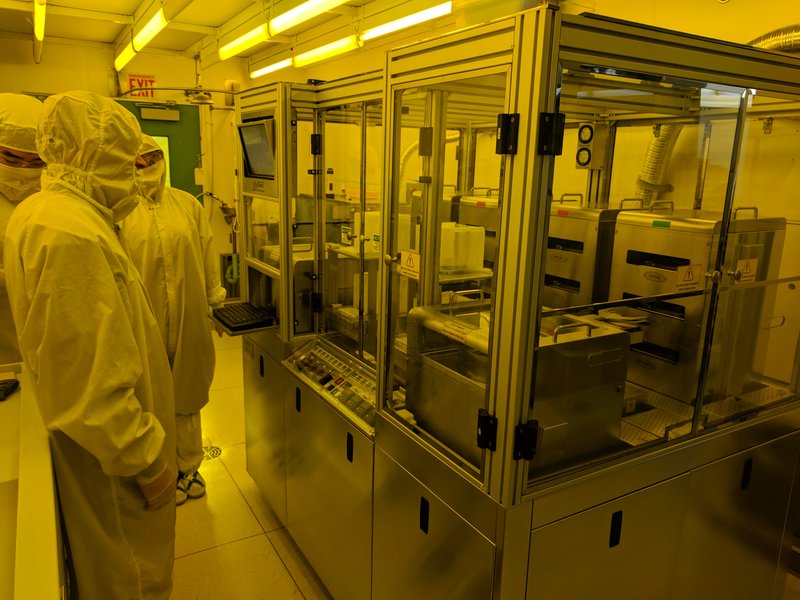
The PicoTrack Lithography system :) Similar to molding and casting, you spin positive or negative resist which is then either weakened or strengthed by exposure.
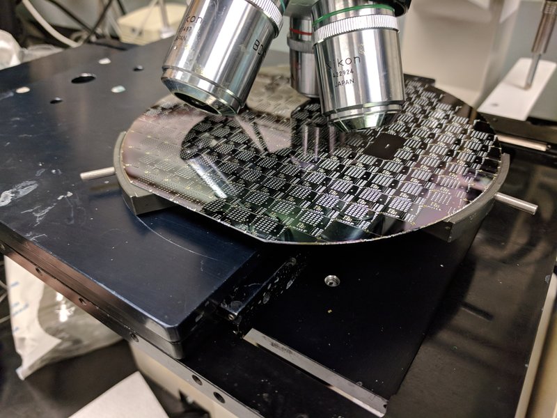
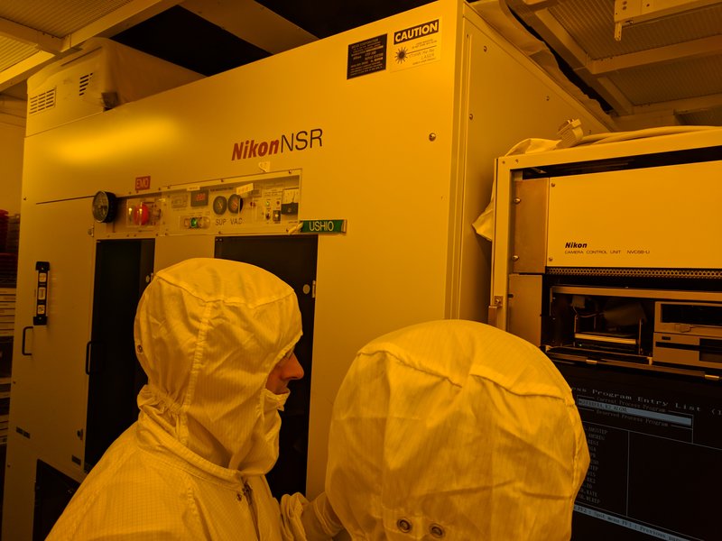
Exposing on the Stepper (to make Metal-Oxide Semiconductor Capacitors, or Contact Aligner for Cantilevers). The cassettes are large masks that are focused to the nano with a large lens.
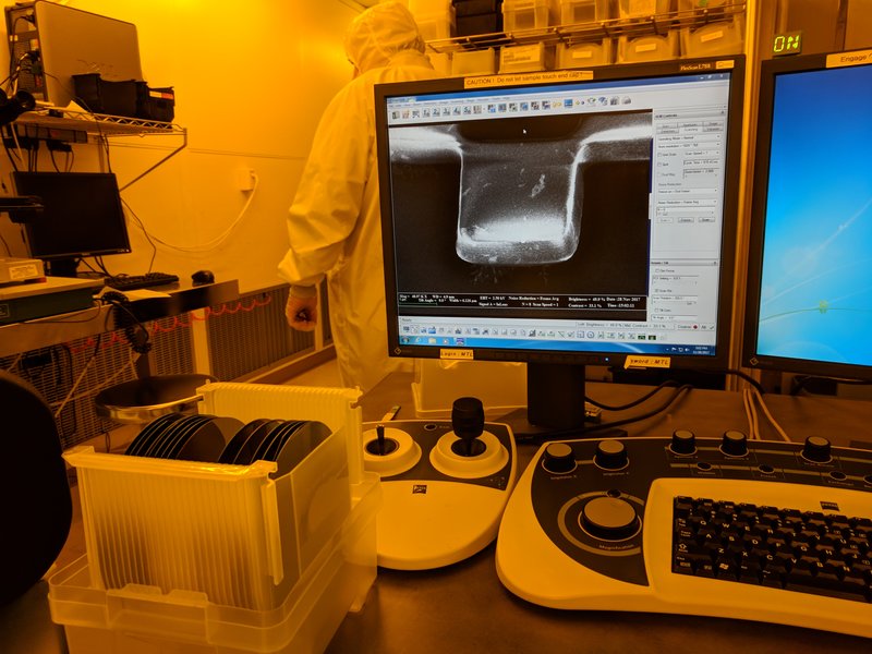
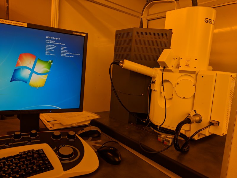
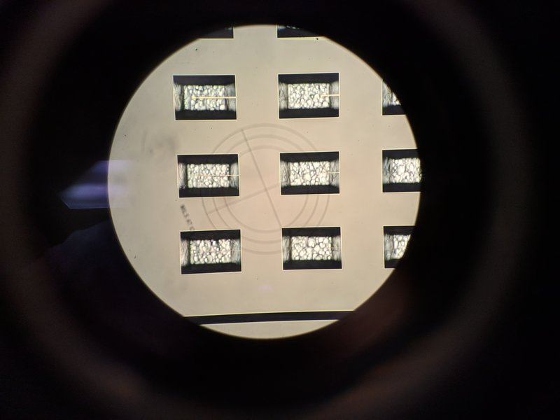
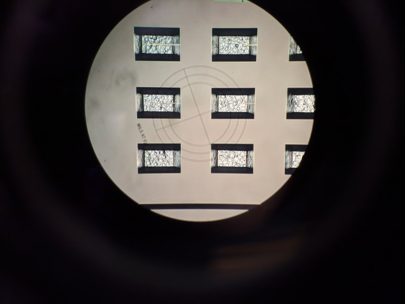
Checking nanostructures with Scanning Electronic Microscope (SEM). The feature displayed is 1um wide! The SEM can resolve upto 1nm.
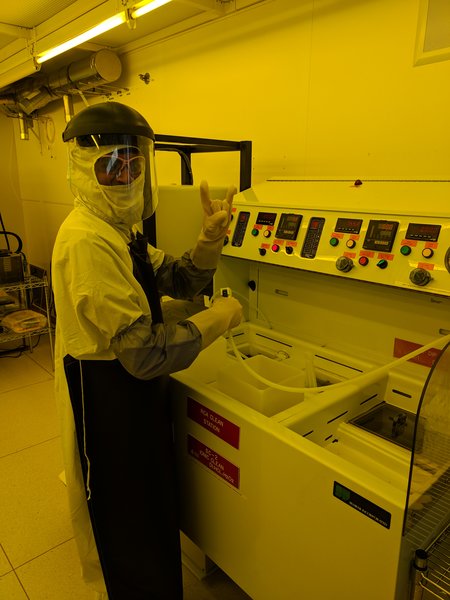
Etching away the metal (Reactive Ion Etch or Wet Etch for MOSCAPs, Potassium Hydroxide KOH etch for AFM Cantilevers). Metal is about 200um below for the cantilever (imagine an empty swimming pool with a diving board).
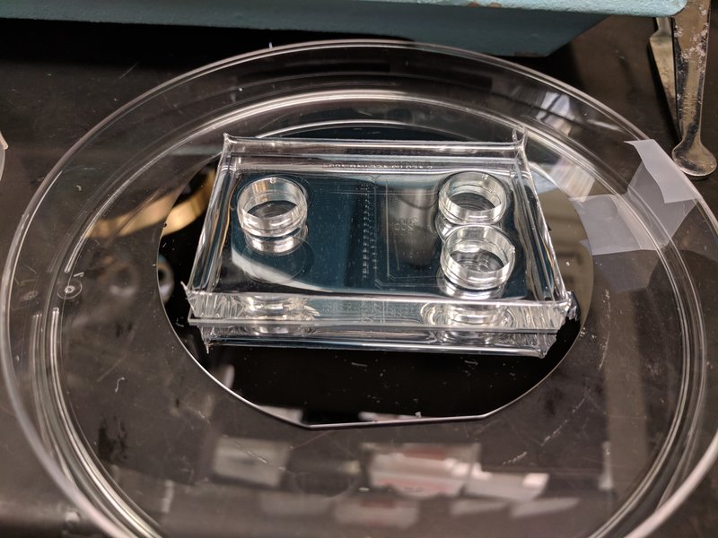
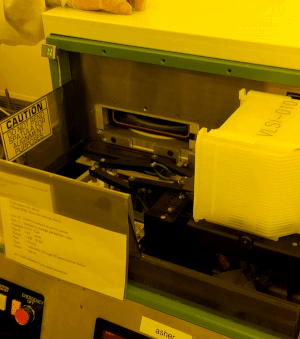
Post-etch with the Asher tool (or you can use Piranha clean). Strips resist on top of metal (or make dangling bonds for micro-fluidic channel).
Special thanks to Scott Poesse our MTL Lab Administrator for taking me through this training.