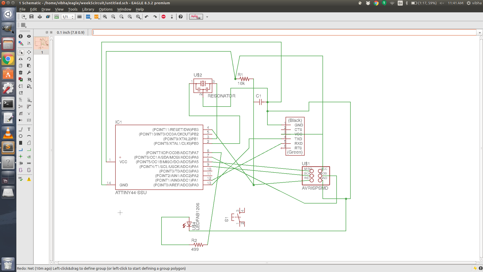
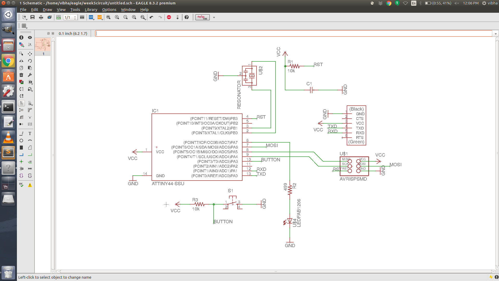
First, I had to download a library of components that I could use in the circuit; these were the items available to us in the inventory. Then, using the "add" button, I placed a few of the components on the board, and using "net", made connections between all the features. Adding the LED and the button was a little tricky, because I had to make sure each of them had a resistor to act as a "pull-up."
Originally, this is what my schematic looked like.
 I decided that although this was functional, I wanted a clean circuit (even though this isn't what the PCB would look like), so I cleaned up the connections. I figured out that labeling two nets connects them, and this was useful in getting rid of lines and in keeping track of what went where. Finallly, it looked like this:
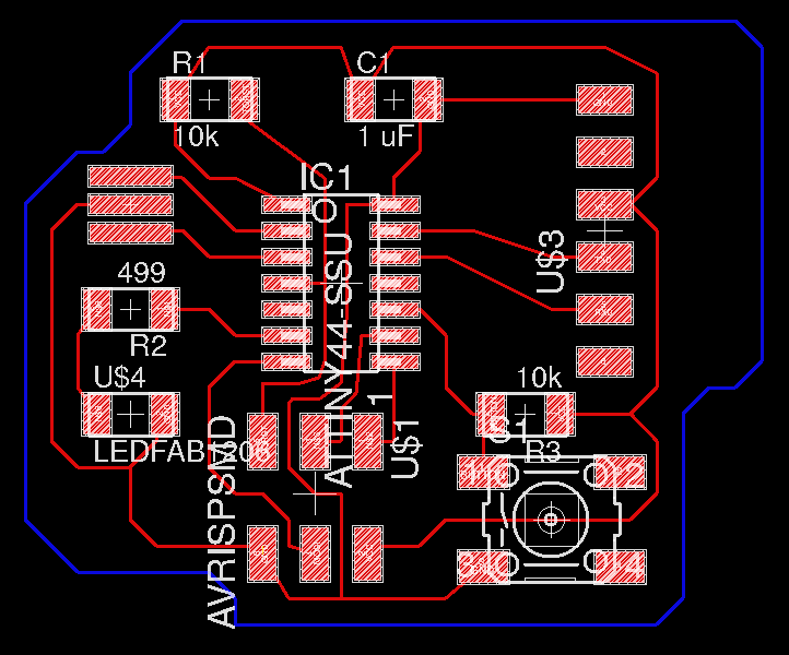
 Then, I made my actual board. This part was tricky, but much easier with the reference diagram we had. I set the trace widths to 10mils and the gap widths to 12mils. The 12mils is too little, and when I checked the vector file for the traces, it was obvious that some parts wouldn't etch out. If I increased the gaps, however, some of my traces wouldn't fit. Eventually, I had to make the minimum gap width 16mils before there was enough space in between traces while still making all the necessary connections. I didn't realize until I was done, but 16mils makes a lot of sense - .0156" or 1/64" or the size of the drillbit is the minimum width for the MODs software to decide a trace is doable, as we found in week 3.
Overall, laying out the board took a lot more time than I was expecting. I even tried autorouting, but couldn't quite get it to work; the traces would be too close together, or there would be airwires or vias. It's a good thing we had Neil's diagram to reference - without it, it would have been an actual puzzle!
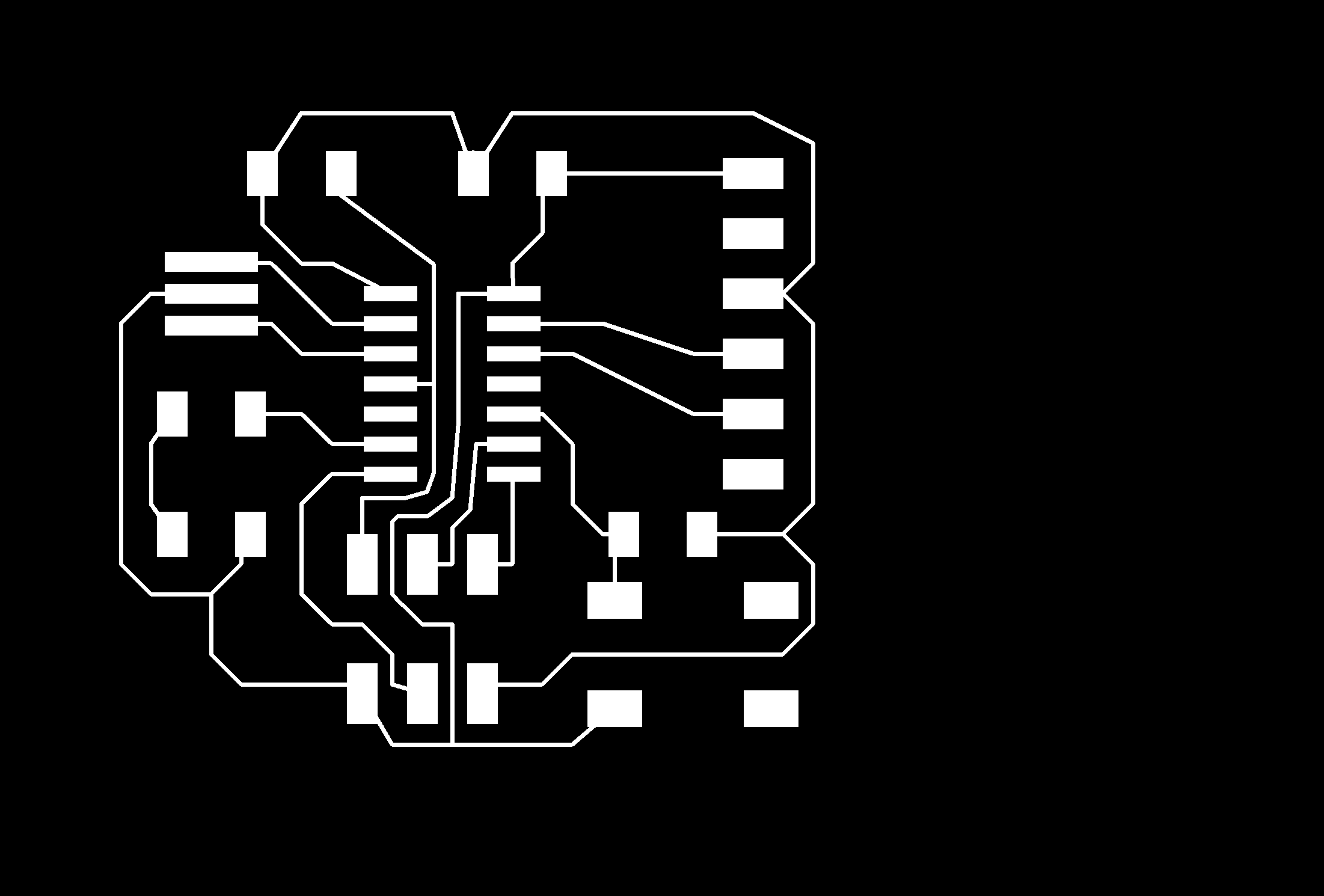
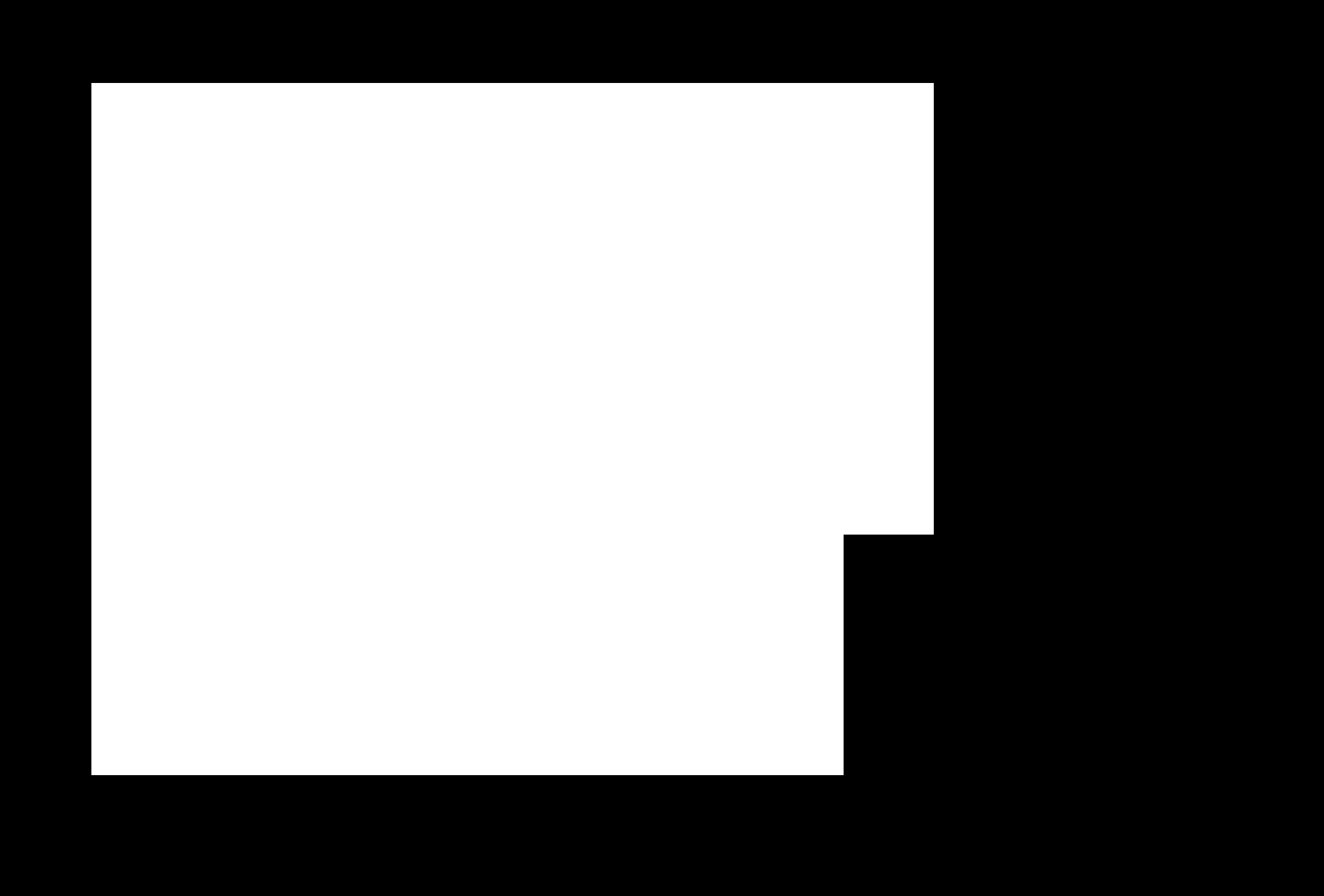
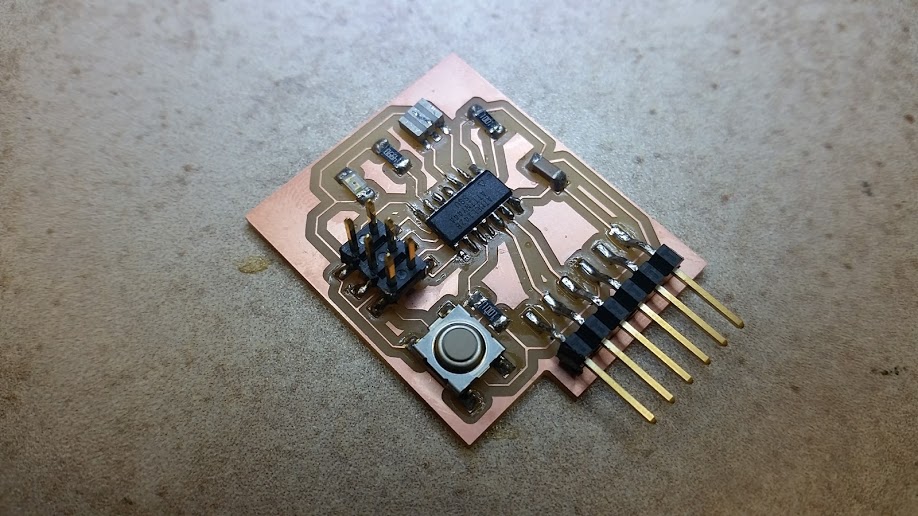
Each time I wanted to check my file, I had to convert the picture. For each of the traces and the edge .png files, I selected only the layer I wanted, set it to monochromatic, and 1000dpi. I used MODs to send it over to the milling machine. The first time I did this, there was a problem with my base; somehow, two outlines were calculated, and so the board was cut out twice in a way that messed up my beautiful traces. After fixing that, the second board turned out great!
Here's what the final .png files looked like:
