Week 4: Electronics Design
"Priyanka Learns HOW TO MAKE a 'Hello World' Circuit Board"
For my fourth assignment for How to Make (Almost) Anything--which involved now actually designing a Printed Circuit Board and understanding the components and its whole functionality--I decided to take a step back and really give myself a crash course in electronic components and printed circuit board design and functionality. I even went back to understanding all the fundamental principles of circuits, so that I was well equipped to be moving forward in becoming proficient on designing circuits -- at minimium at a hobbiest level. From there I (slowly) went along with the assignment and satisfied the requirements as best as I can. The following sections lays out what occurred for this week's assignment.
Individual Assignment: Recreating an Existing hello_world Board + Adding Additional Components
Since I currently have limited knowledge of electronics and electronics design (though I am excited to learn because electronics is super cool!), I decided to be very methodical in my approach to this assignment. I first had to get a grasp of electronics schematic and board design layouting and I decided to use Eagle as my first PCB design software to try.
First off, I have very minimal background in electronics and electronics design (but I think it is super cool!) and also my first experience with PCB CAD with EAGLE, so it was quite a steep learning curve, but learning a lot along the way!
First, I learned how to download the FAB components library (fab.lbr) into Eagle from the cba gitlab repository.
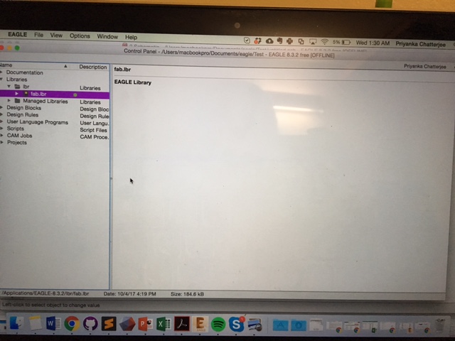
Figure 1: FAB Library
Then I started getting used to finding the right components in the library, learning all the component names, and understanding their functionalities.
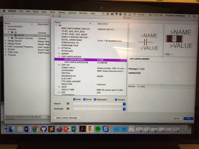
Figure 2: Learning How to Add Parts onto EAGLE Schematics
Below is a picture of my first attempts at using Eagle and making a really simple circuit schematic:
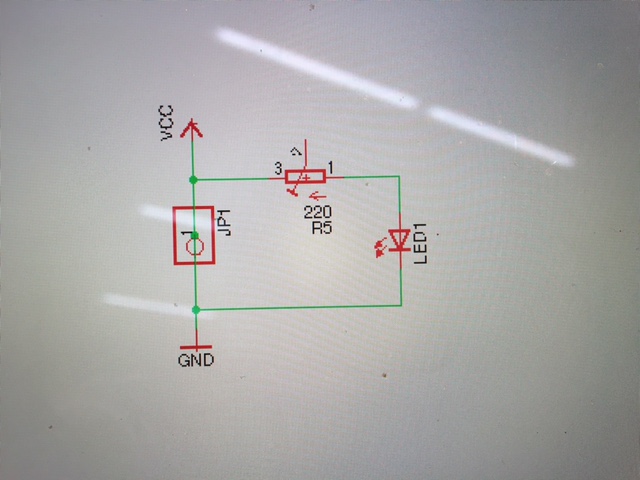
Figure 3: Practicing at Eagle - Schematic Design
Once I got more used to Eagle, I continued to gain more proficiency and then got started on the assignment. The assignment requires us to design and fabricate a printed circuit board that blinks an LED with a switch, working off an existing hello_world board --> with the design given to get us started.
The schematic and component information given to us are as follows:
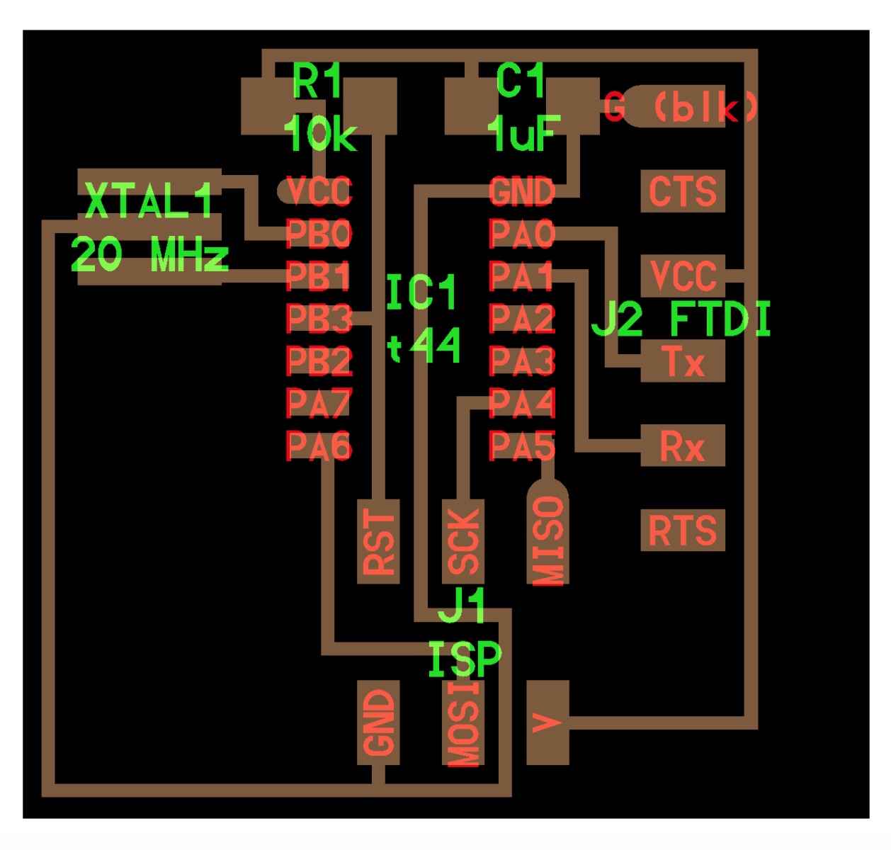
Figure 4: Given Layout
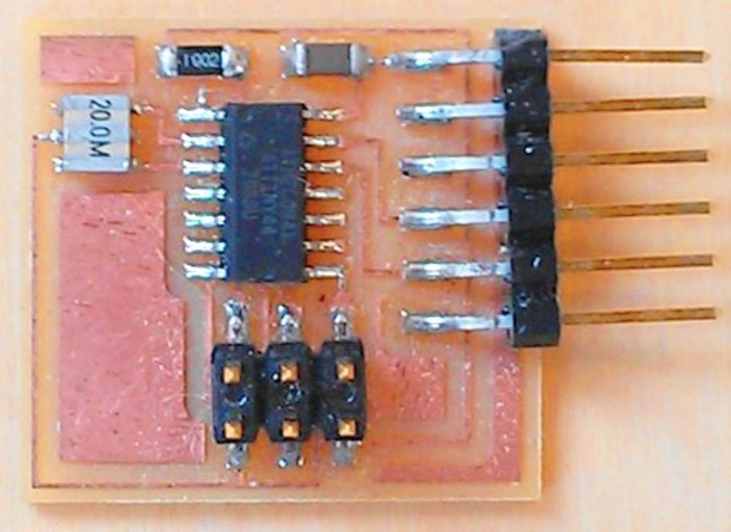
Figure 5: Given Components (To Start With!)
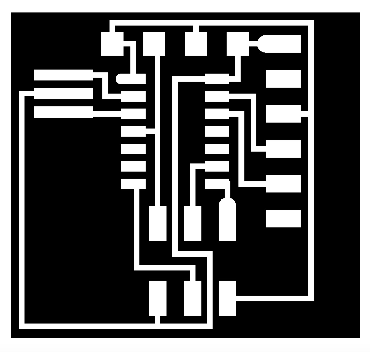
Figure 6: Given Traces
The components that I have decided for the design are as follows:
PCB Components
6-pin Header 10k Resistor (1) 1 uF Capacitor 1K (Voltage Regulating) Resistor (1) J1 ISP 2x3 Connector SPST-NO 0.05A 24V Switch Tactile Button 20 mHz Resonator Red Clear 1206 20mA 3.3V LED
Here I am getting started with Eagle and putting down components that look useful:
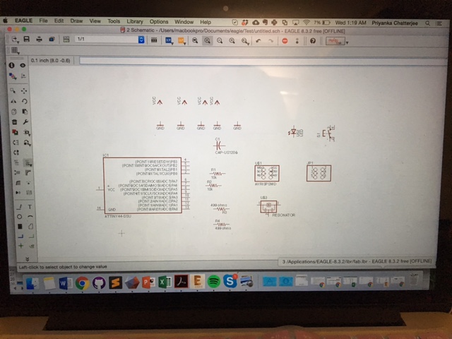
Figure 7: First Try at Putting together Schematic Components
Next, I plan to put together the PCB layout with the schematic components with the proper connections and then actually milling out and stuffing the boards with the actual physical components themselves. Pictures to come!
UPDATE!
Back to Electronics Design! Through the process, I consulted with several amazing EEs who really helped me out learning about everything electronics, how microcontrollers work, which pins do what, and what components they go to, etc. It was a steep learning curve, and I'm still running uphill, but it is all really liberating and empowering!
First, I went back to the (practically literal) "Drawing Board" on EAGLE and started arranging my components properly and then routing traces to them. But first! As per my friend Apoorva, a REALLY long-time student and now Postdoc at MIT, I needed to first read the datasheet of the ATTiny44A microcontroller that I will be using. In the datasheet, I will learn what each of the pins are supposed to go to and what components need to be routed to them. I first took a look at the pin configurations and learned what each pin allows me to do and control. Very cool stuff!
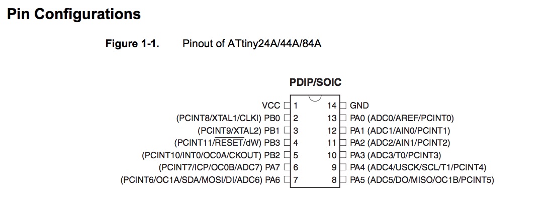
Figure 8: Pin Configurations from the Data Sheet of the ATTiny44A Atmel Microcontroller
Here below are the components that I used for designing my board for this week's assignment:
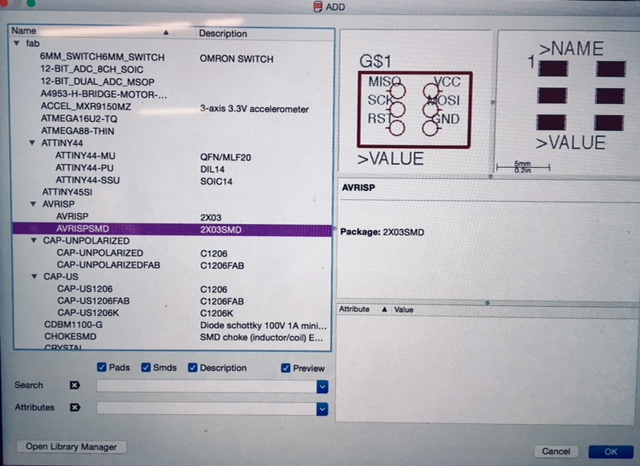
Figure 9: ISP Header - Schematic Component
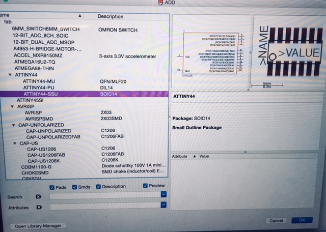
Figure 10: ATTiny44A Microcontroller - Schematic Component
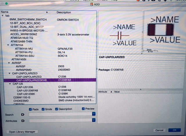
Figure 11: Capacitor - Schematic Component
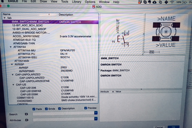
Figure 12: Omron Switch (Button) - Schematic Component
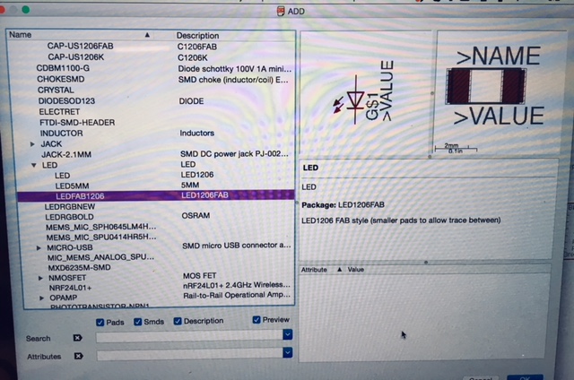
Figure 13: Green Clear LED - Schematic Component
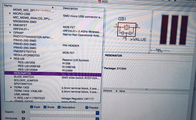
Figure 14: Clock-Setting Resonator - Schematic Component
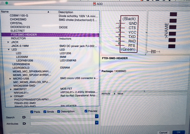
Figure 15: FTDI Header Pins - Schematic Component

Figure 16: Resistor - Schematic Component
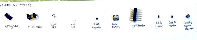
Figure 17: Picture of the Actual Components Themselves that I Labeled so Convenient for Me to Find for Stuffing my Board
Once I was confortable with understanding the datasheet and how the ATTiny44A (sorta) works, I took some tips from Ben Yuan and Alex Kaspar in my class, and learned, through their work, how to effectively route the pins to the various components (above) for my board. Here below is the progression towards my final schematic that I made in EAGLE, and then below is the actual layout with Routing Marks (where no component traces are crossing, yay!) that is what will be milled out on the mini mills to make my board. Big thanks to TA Shireen for helping me work out the kinks!
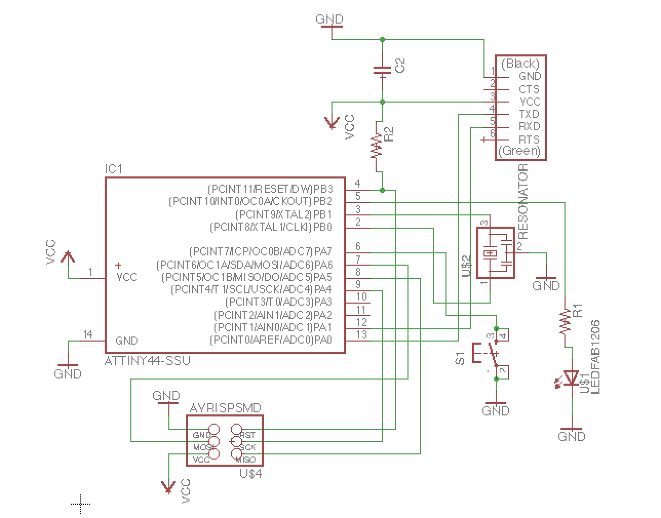
Figure 18: Final EAGLE Schematic for my "Hello World" Board with LED + Button
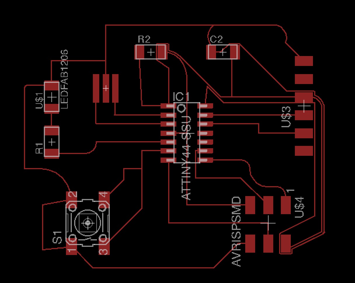
Figure 18: First Layout Try (With really weird looking traces, some too close together, too)
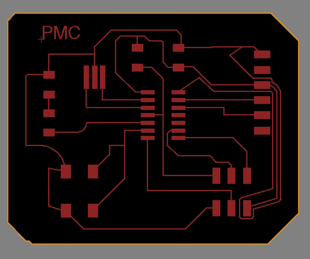
Figure 19: Final EAGLE Board Layout for my "Hello World" Board with LED + Button
I then converted these .sch and .brd files into PNG picture format, so that I can then export them into the mini mill software to produce my board!
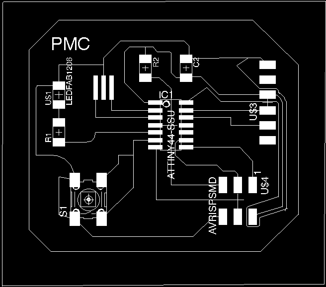
Figure 20: PNG File of My Board!
It turns out that the mill I was using the "OtherMill" doesn't need a PNG format, but instead just works off of the .brd layout from EAGLE directly. However, I did come up with several glitches before the final design was milled properly. First, I added an extra outline and then milled not only the traces but ALSO the outline(s) with the 1/64th endmill. Even before that, I was getting error messages that my traces were too small because I didn't switch my endmill size from 1/32 (the size I will be using for just the outline cut) to the 1/64 size for tracing. When I finally got the mill to start, I also realized that not only was my outline getting "traced" but I forgot to properly position my board layout on the software interface, and so accidentally milling into the mill bed itself (yikes!) and damaging the 1/64 endmill. I also didn't get the traces with sufficient thickness (and too much clearance) and so produced a board with very thin copper tracings, which would make the board vulnerable to shorting once in use. Here below are some of the flubs:
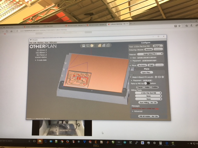
Figure 21: Bad Traces --> Too Close and Accidentally Indicating a 1/32 endmill when it should be a 1/64
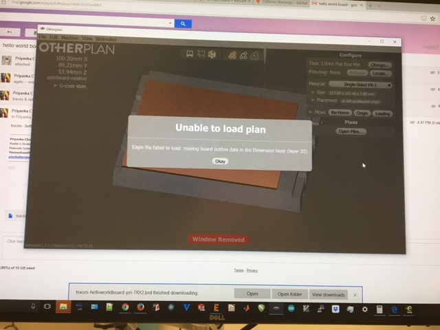
Figure 22: The Other Mill cannot read my File Format
However, once I actually did get the board to be milled, it nevertheless became an issue, due to the bad end mills that I was using -- which was basically ripping into the copper substrate, instead of cleaning milling it out. Here below is a consequence of that:
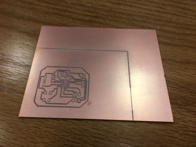
Figure 23: Poorly Traced Board
I finally was able to mill out the board successfully (with a triangular-pointed endmill and with the proper trace widths and spacings and feeds and speeds on the machine)! I then finally completed the assignment by stuffing on the components and completing the board.
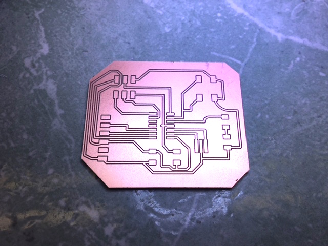
Figure 25: Successful Cleanly-Milled Board
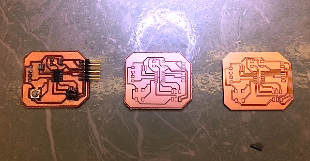
Figure 24: Comparing all the Boards Milled
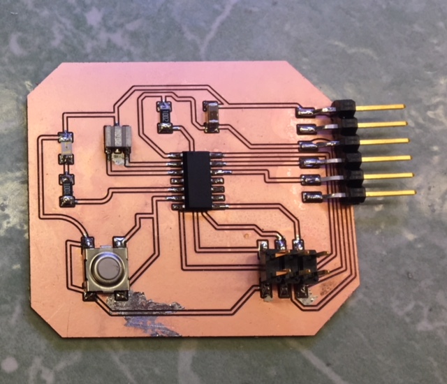
Figure 27: Finished Board (some (fixed) Solder Errors and thankfully no shorts)
Whew!! This (very long and many-times arduous) experience was all in the end really eye-opening and made me feel really knowledgable and powerful, being able to put together circuit boards. I am now filling in the gaps of my engineering knowledge (slowly but surely) and do see myself using these skills moving forward.
Final Project Preparation: Aligning Desired Capabilities with PCB Requirements
The goal for my final project is to create a "comfort enhancing" multi-display multifunctional shoe that conforms to my foot and changes color through an LED array display. The goal will be to manipulate "soft actuation" devices within the shoe's internal lining via signals from a Low-Power (hopefully) Bluetooth device that syncs with an app on your phone. There will also be other signals to change the color of an LED array on the outer shell of the shoe that the PCB needs to satisfy. I want my shoe to be a mini-computer with piezoelectric devices for pressure sensing and actuation caused by expanding and contracting gel-filled pockets. I am also considering including shape memory alloy devices as aonother subset of output devices for the shoe. This will be fleshed out in more detail during the Output Devices week!