Milling PCBs and Soldering Surface-mount Electrical Components
This week our task was to make a Programmer. A programmer, as described by Wikipedia, is an electronic device that is used to configure or "program" an integrated circuit. The programmer we made this week will be used in subsequent weeks in order to program PCBs and circuits we design later in the course. This week, the focus was primarily getting the fabrication method down.
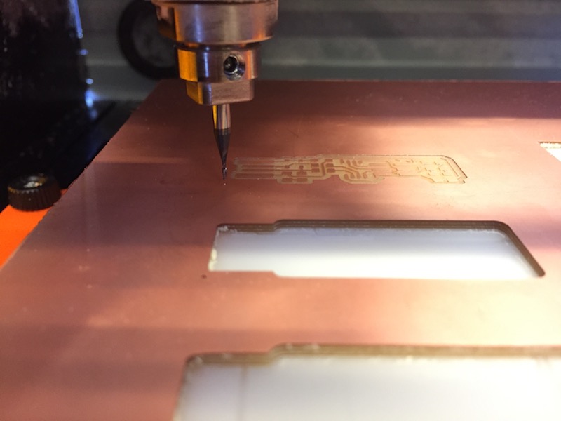
The goal of the week was to learn how to make our own printed circuit boards (PCBs) by taking a PCB blank made of a layer of copper over phenolic paper and milling out the copper that we don't need until the proper circuit traces are left behind. In short, we want to turn...
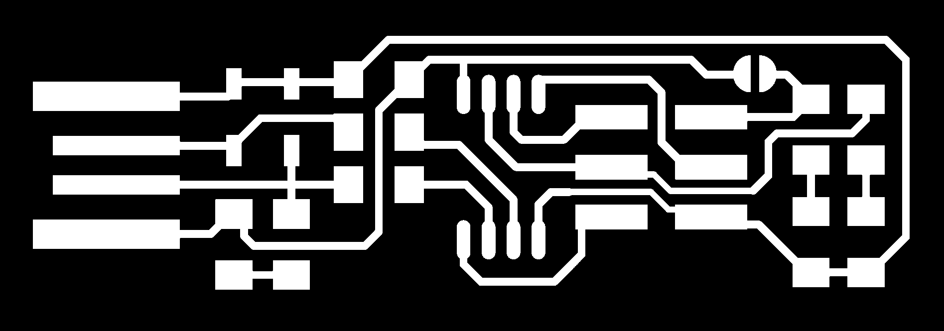
into...
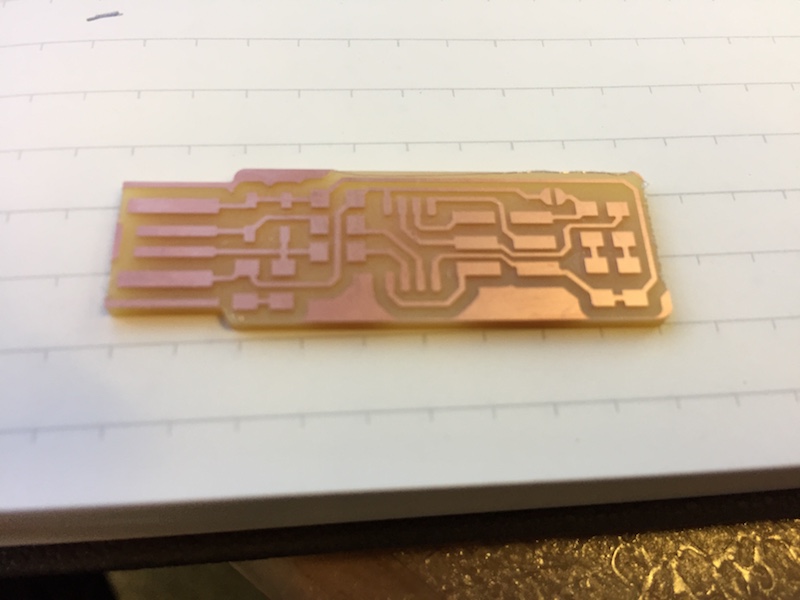
and finally into...
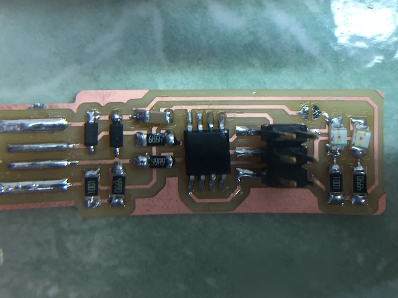
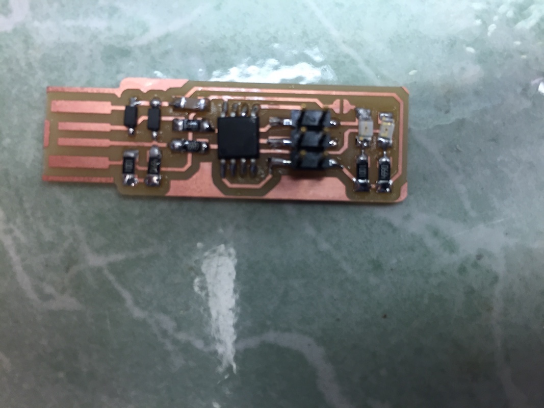
(Yes, I know that is not the greatest soldering job in the world)
Milling PCBs
The first step in making a custom circuit board is to get rid of the copper on our PCB blank that isn't part of our traces. So, in essance, we want to remove the inverse of the traces of our circuit. Examining the images above, the white part is our circuit traces, so we want to remove the copper that exists in the black parts of the image.
To remove the copper, I used a Mini CNC Mill (the Roland monoFab) to remove the copper from my PCB blank. The CNC Mill was controlled by similar open source software (MODS) written for this class as the vinyl cutter. The software (pictured below) took as input a picture of the traces, and performed some image processing to produce cutting lines that the CNC Mill follows.
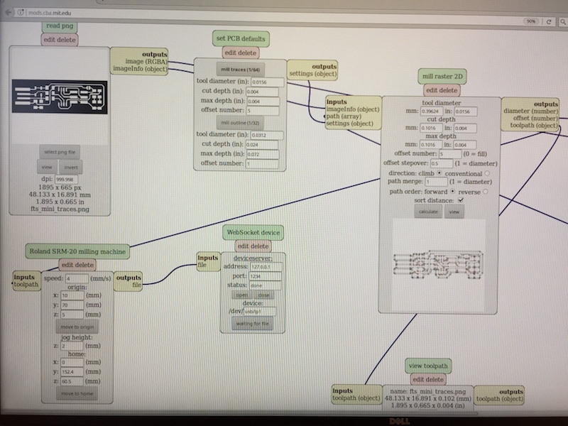
The steps were as follows:
- Choose the image with the traces for your circuit design.
- Choose "Mill Traces" and set the proper offset number (usually 4 or 5). The other parameters including cut depth should be fine with the default values. Make sure the mill has the proper bit installed.
- Click "Calculate" on the third program window pane to generate the trace cuts.
- Set the origin of the mill manually to where the bottom left of your circuit design will go. To set the origin, move the mill bit very close to the PCB over where your bottom left corner should be. Move the mill bit by adjusting the X, Y, Z parameters and then clicking "Move To Origin." Loosen the bit, let it fall to the PCB bed, then re-tighten it. The origin is now set.
- Open the server socket, re-calculate the traces (make sure they're what you expect), then send the file to the printer and watch the machine do it's job.
My experience creating my first PCB was actually very nice. I didn't break the mill bit like we were warned we would almost certainly do if we didn't follow instructions. One problem I ran into was the mill bit not cutting deep enough into the copper on the right side of my circuit design. What I did to fix it was push the PCB blank down harder onto the sacrificial layer of the mill. Since the PCB blank was stuck on with double-sided tape, it's very easy to have a slightly uneven surface. So make sure the bed is flat. Additionally, I re-loosened the mill bit, and held it pressing on the copper bed while I tightened the shaft screw. My TA believed that sometimes when tightening the shaft screw, the mill bit can lift a little off the copper bed, so make sure it's touching the copper before starting the cut job. Between both of these fixes, the second round of cutting worked fine.
The next step is to cut out the PCB. This is a very similar process to cutting the traces:
- Change the mill bit to be the appropriate diameter (usually the bit to cut out the board is bigger than the one to cut the traces). Note: Don't change the origin of the machine, or if you do - make sure you remember the X and Y values of the old origin. Either click "Move To Home" or just increase the Z value to change the bit.
- Choose the image with the outline for your PCB board.
- Choose "Mill Outline."
- Click "Calculate" on the third program window pane to generate the outline cuts. Note: This should be a 3D rendering with cut lines at different Z-values.
- Open the server socket, re-calculate the traces (make sure they're what you expect), then send the file to the printer and watch the machine do it's job.
And Voila! If everything went right, the board should be loose and have cut through all of the phenolic paper layer under the copper that makes up the bulk of the PCB.
Soldering Surface-mount Electrical Components
This is where the fun begins. If you've never soldered before, you definitely want to practice soldering through-hole components before moving onto surface-mount components. I practiced with some through-hole resisters and protoboard before trying to solder the surface-mount components onto my board.
I've found that there's both a science and an art to soldering at this small surface-mount scale... There are some tips I learned along the way that would've been nice to know up front:
- Use a small-tip soldering iron. Trust me this will increase your control and precision by many factors.
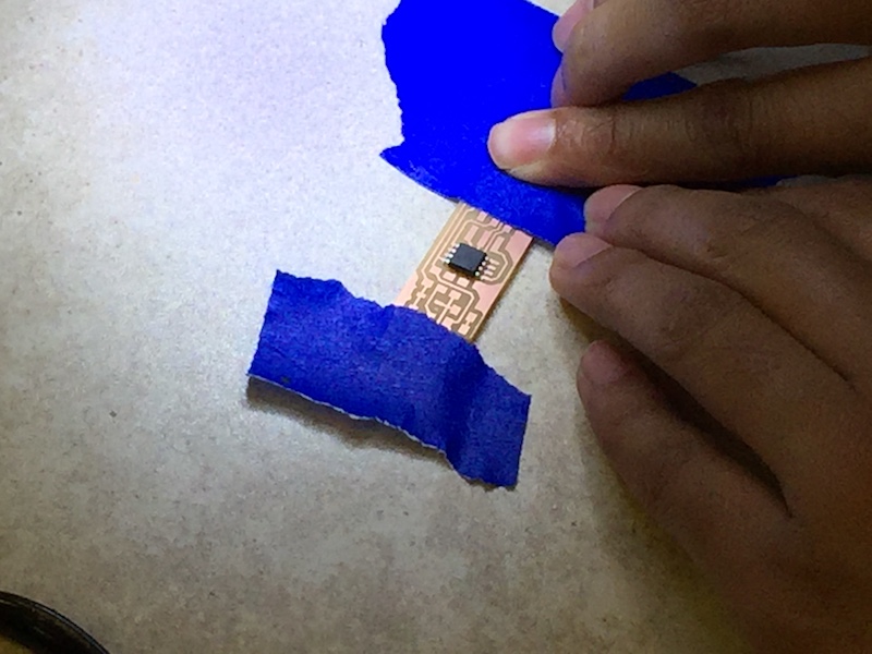
- Tape your board down to your workspace so you don't have both the board and electrical components moving when you're trying to solder. (Thanks to Nikita Waghani for the tip!)
- Soldering the first joint of any component is by far the most difficult part. A neat trick I didn't learn about until after I was done soldering my board is that you can put a little bit of solder on the patch of copper that the first lead will attach to. After the solder is already in the right position, heat it up with the soldering iron and mechanically place the component onto the solder patch in the right orientation, then let it cool. This won't generally be a good connection, but it'll be stuck in place for you to make a good connection on the other lead(s). Then come back to this joint and resolder it once the other leads are in place and have good joints. (Thanks Ben Yuan for the tip!)
- Start from the middle of the board and work outwards. It's easier to get your soldering iron in the right place when there aren't other components in the way.
- Go component by component. Resistors all look the same at this scale, particularly when they're 49.9 ohms and 499 ohms. Trust the packaging, and don't get your components mixed up.
- Use a magnifying glass or lab telescope to see your board more clearly.
- Be careful about components with polarity (i.e. diodes, LEDs, integrated circuits, power supplies, etc.)
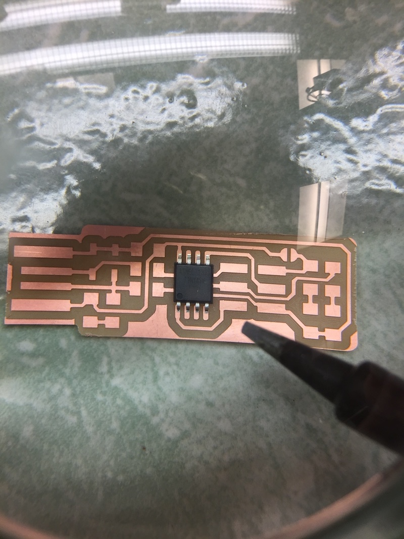
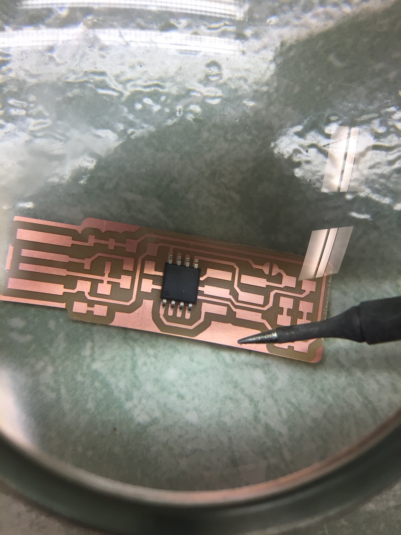
I found that after doing a couple components, I got into a type of zen state where I got pretty good at making good solder joints for the tiny electrical components. When I was finished with the board, it looked like so:
Programming the Board
The last step in this process was programming the board. As I said at the beginning of this post, the task of this week was to make a programmer. But before our board can act as a programmer for other boards, it itself has to be programmed. In all honesty, I'm not super familiar at this point what exactly is happening when we "program" the integrated chip (ATTiny45). This is starting to get into circuit theory that I am not familiar with, but this will come with time over the next several weeks. For now, I was religously following this tutorial and using an existing programmer to help program my circuit.
Some problems I ran into included not having even amounts of solder on the part of the board that connects to the USB connector. The two larger outer leads are for ground (GND) and power (VBus). The two innter leads are for data transfer. All the leads had to have consistent and solid contact with the USB connector in order to reliably be programmed. So I spend several attempts to get all four of the USB leads to approximately the same height. If you recieved any of the following errors,chances are that you need to redo your USB solder connections.
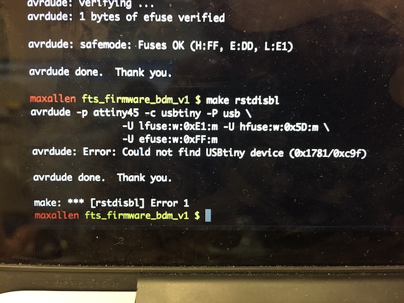
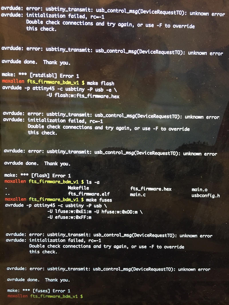
If you're still running into problems, it might be time to take out a multimeter and start debugging your circuit. I used a multimeter to check both the power and ground USB leads. I measured something around 1.2 Megaohms. Really what you should look for is when the resistance is zero or significantly lower than what you expect. This might indicate that you have a short circuit and plugging it in could cause magic smoke.
If all goes well and the software instructions are executed properlly, you should have a functioning programmer as soon as you desolder the Vcc and Vprog pins as talked about in the tutorial. Final product:
Update: The programmer worked to program another programmer and board, although because of the USB solder connections and some of the solder connections on the ATTiny, the programmer was pretty unreliable. I ended up making another one after I had practiced soldering more...
Terminology
Programmer, circuit traces, phenolic paper, board house, magic smoke, through-hole, surface-mount, soldering
Technologies Used
Roland monoFab SRM-20, Soldering Iron, Programmer