Double-Sided Sticky Tape
Ah yes, double-sided sticky tape, the true MVP of the week. But I'm getting ahead of myself.
During the training session, we learned how to afix the boards onto the sacrificial layer and set up the mods program to trace and cut the machine. As I later learned during my attempt to mill my PCB blank, it was really important to push down quite hard on the board after afixing it with double-sided sticky tape.
We started out by characterizing the machine. Julia, Jordan and I were able to mill the pattern provided and achieved pretty good results. Although the tip was unable to carve out a section by about 0.020 in the diagram, it was able to create a section much thinner. This will be important for when we design our own circuit boards.

Next, I tried milling the actual design from Brian. I added double-sided sticky tape to the board and pushed down firmly. Upon looking at the board from the side, I realized that it wasn't exactly flat. Although the center of the board was flush to the sacrificial layer, the edge, which did not have enough tape, was maybe 1mm off of the sacrificial layer. I removed the board and applied more tape the that edge and also gently bent it towards the back. I reapplied the board and this time it looked okay. I adjusting the cutting tip to sit snuggly on top of the board. This is what the milling process looked like.

Comparing with the demo piece that was cut out for comparison, I wanted to remove some more matieral to make the soldering process a bit easier. I ended up using 7 traces instead of the recommended 4, but I probably could have gotten away with 6. After this milling, this is what my board looked like.

I noticed that some areas were improperly milled, and that there were still bits of copper left on top of the board where there shouldn't have been. Since they occurred throughout the board, I felt that it might have been because the tip was dulling. I decided to try milling over the same area without changing the origin with a new tip, which worked nicely. Dixon also recommended that I could have tried re-milling with the same tip, but setting the machine to remove slightly more material. He said that this is more economical as this prolongs the lifetime of a particular tip. As a result we kept both tips, but made a note of which one was older. I will keep this in mind for the future.
Once the traces were finished, I cut out the piece with the thicker tip, and had no problems. Dixon also gave the good tip of sticking a thin metal ruler in between the cut out part and the leftover board to remove the piece without affecting the scrap piece too much. Previously, I had just pried the whole board off to remove the piece, but Dixon's suggestion prevents significant warping of the leftover board. The unused portions of the board are basically already set up for additional cuts. All that needs to be changed is the origin.
Now that I had my blank PCB, I was ready to solder. During the training, Rob mentioned that we needed to be careful with the solder waste because it contained lead. It was also a rosin core solder, which meant that we technically shouldn't need additional flux while soldering. He also demonstrated the proper techniques to desolder with a braid and a heat gun. I practiced how to tack down one pin of a microprocesser a couple of times before I attempted to solder my own PCB. I quickly found out that it was difficult to get the solder to stick to the surfaces and pins. I attempted to clean the soldering iron clean, but every time I brought in the solder, it would just melt onto the tip of the iron and not want to stick to the copper surface.
I did some searching on the internet and found that this is due to the formation of the oxide layer on the metal. I added some liquid flux to the surfaces just before soldering, and that helped a lot. I also moved to solder under the microscope, and that made it much easier for me to see what I was doing as well as to asses my work. I collected all of the parts that I needed beforehand as Rob suggested and arranged them on an index card with, you guessed it, double-sided sticky tape. I also set up my soldering station.


Following the instructions on Brian's page, I soldered the ATtiny first. This was the result.

I was fairly satisfied with the results. The solder was shiny, as Neil had mentioned was necessary for a good join. I felt that I might be using too much solder and the joints were a bit irregularly shaped, but good enough for now. I continued to solder, making sure I followed the orientation of the parts given on Brian's circuit diagram. An important thing that I realized was that LED's are diodes and that they had a direction as well. Luckily, I realized this and was able to check before soldering them.
Things went pretty smoothly for the most part. I needed to use the solder braid a couple of times to remove excess solder when I flooded a few copper pads. Painting the end of the braid with some rosin before bringing it to the solder I was trying to remove helped a lot.


I also needed to desolder one LED after the solder kept solidifying into the crystalline or sandy texture that Neil had warned us against. I had already applied too much solder and it was just aggravating the problem. Flux did not help much either. I decided to remove the LED and try with a new one as it seemed like the crystallization was being triggered by the existing texture.
In this image, I have the LED that I desoldered under the microscope. The right side shows the side that had a good join that was shiny and smooth. The left side was the problematic side that kept crystallizing as the solder solidified. Someone suggested that maybe it was cooling down too quickly, or that I wasn't warming the pad up enough before adding the solder. I'm still not sure exactly what went wrong here.

After switching out the LED, I was able to solder the rest of the PCB without any major issues. I ran into a similar problem with soldering the bridge. The first one shows the solder with the dull texture. I applied some flux and re-melted this and achieved the result in the second picture.


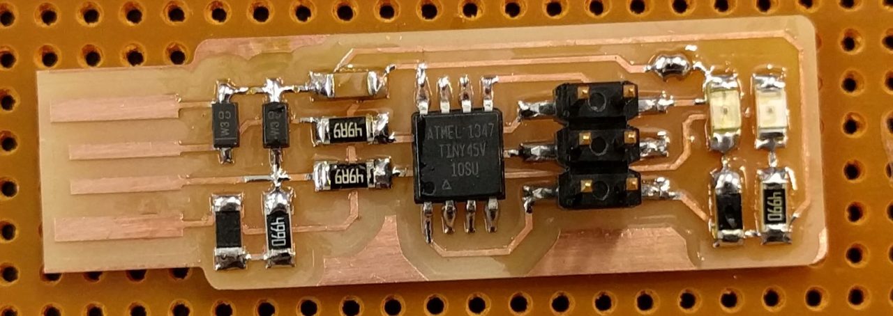
This is the PCB before I tried to program it.
Next, continuing with the directions from Brian, I added a layer of solder on the USB connection and attempted to connect it to the computer to program it. The connection was a bit finicky, so Rob suggested that I add a layer of tape on the back. This made it work much better. After some initial uncertainty with the orientation of the 6 pin linkage, I was able to get a working connection. After connecting it to the USB on one end and the programming ISP on the other, I ran the command make flash followed by make fuses on the lab computer which already had the make files set up. After this I checked the USB functionality and desoldered the bridge and ran make rst disbl. Afterwards I tested to see if it was functioning as a programer by using the avrdude -c usbtiny -p t45 command in the terminal. All seemed to be going well.
Here is the final result:

Special thanks to Dixon and Rob for their help and insight!