Mouse and Eagle
One is insufferable without the other.
The goal for this week was to design and create our own PCB based on designs from Neil's template. After downloading Eagle and importing the fab library into it at the section, I was ready to design my PCB. My initial attempt at laying out the PCB in Eagle failed miserably as I did not have a mouse with me! It is basically impossible to do anything in Eagle without a mouse. I was unable to drag the view and kept scrolling accidentally which changed the view dramatically. I gave up until I was able to pick up my mouse, and that worked a lot better. I really appreciate how after you add a componenet, Eagle takes you back to the adding menu so you can add all of your components at once. Dixon and Rob gave a lot of tips, such as making sure to move the layout close to the origin before exporting as an image, using thicker than the default traces, and exporting as a monochromatic image. Using Neil's and Rob's example PCBs, I was able to design my own.
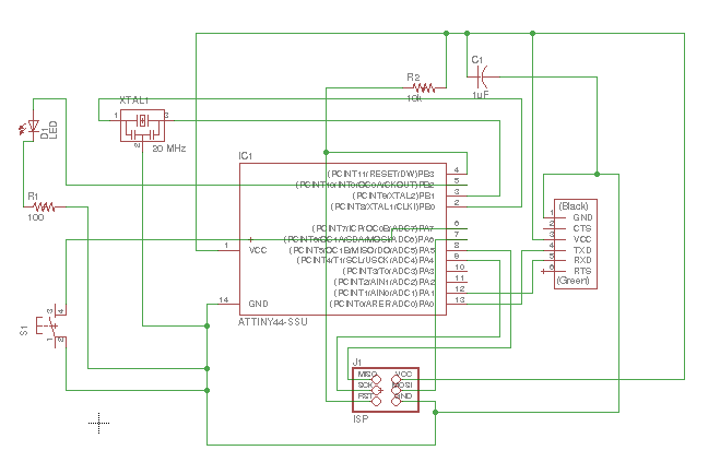
After double checking that all the connections were correct, I began to actually design the traces on the board. This was slightly more annoying than expected, as moving the components was a nontrivial task. First, I didn't realize until Julia mentioned that we needed to click on the "+" icon in order to move individual componenets. Previously, I had tried to just click and drag from the center of the component, but that was not correct. Next, in order to move a group of components, you needed to use the "select" tool from the toolbar to group different components together, then change to the "move" tool, then right click somewhere on the grouping and select move group before you can move it. If at any point you mis-clicked, which I did, you had to restart at the beginning. This led to some frustration, but I was eventually able to move all of my components to their desired locations.
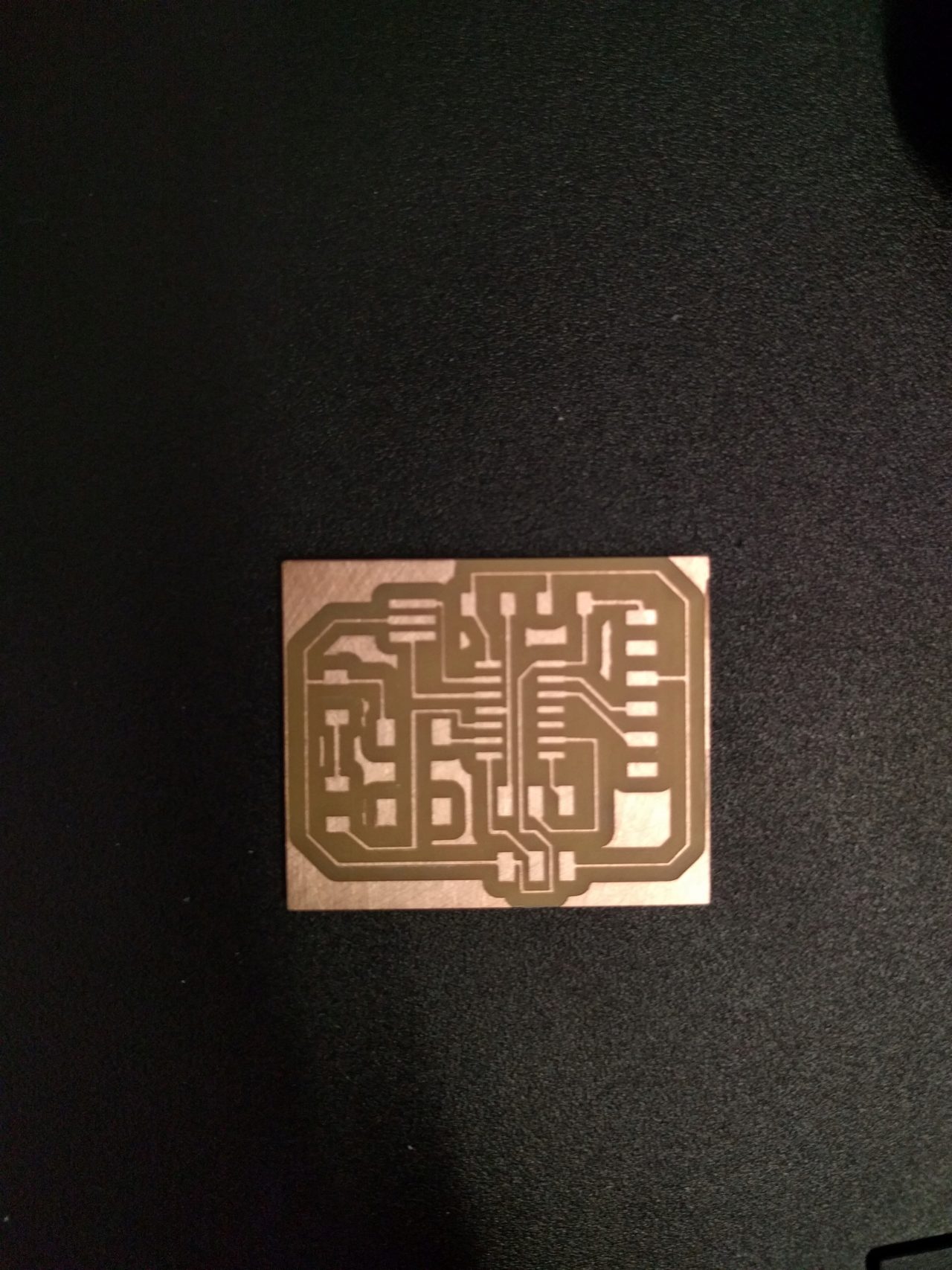
Connecting the components was admittedly a lot of fun. The software did a good job of showing you where you still needed to connect by drawing a yellow line from one connection to the other and updating to follow your trace. It also would highlight all the pieces that needed to be connected to each other if you clicked on a particular pad for a component. However, the traces that it would let you draw were often oddly spaced. This led to problems where there were large spaces on the PCB that were not accessible because the trace had to move a set amount outside of the pad. Some traces were therefore closer together even though there was space to separate them. I'm still not sure if there is a good way to deal with this issue. In the end I was able to create a trace that looked pretty decent.
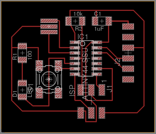
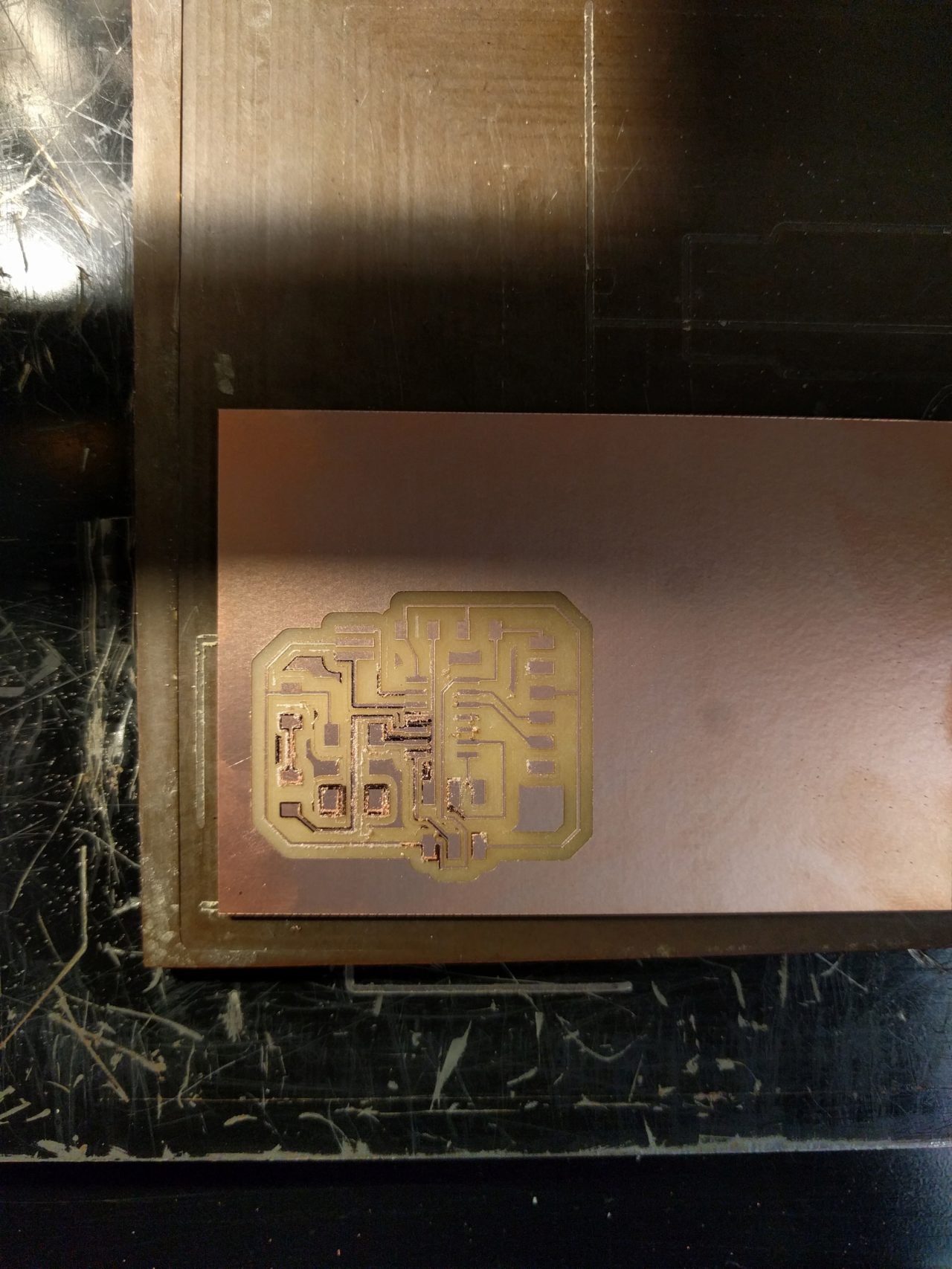
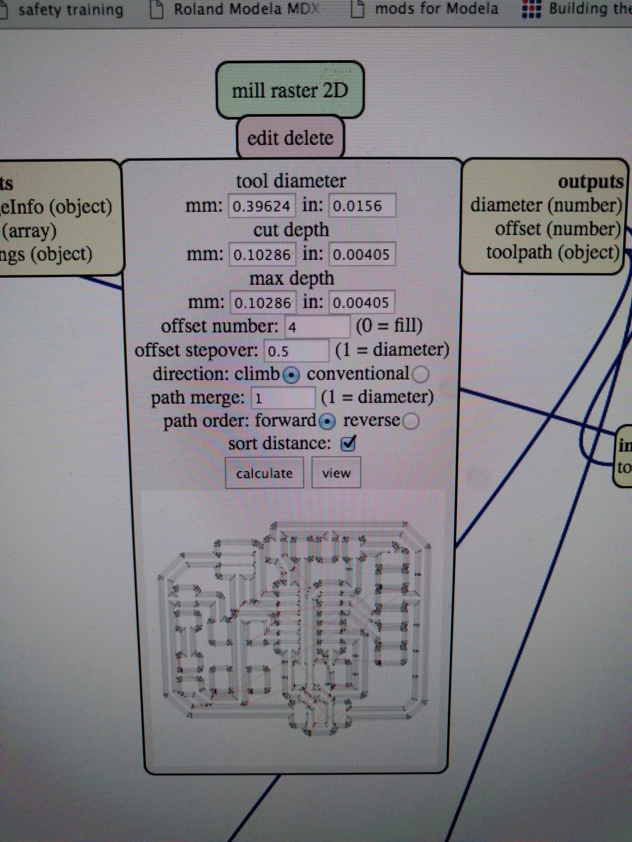
After I exported it as an image and created the outline for it in paint, I took it to the PCB milling machine, and upon checking some of my traces were indeed too close together. Although we had characterized the machine, I still didn't know what the units looked like on the board schematic, so I had to thin the traces by trial and error until I reached a thickness that allowed me to mill around everything. This took about 3 tries, but I eventually settled on a width of 10. In the future, I think I'd like to try 12, as I ran into some problems which I will mention later. For now, I was able to mill the PCB. The first pass resulted in something quite similar to a previous failure I had had with milling the USBtiny PCB. I decided to use Dixon's suggestion of milling a bit deeper on a second pass, since it was mostly successful except for some spots around the edges. An important note, when changing the cut depth, make sure the max cut depth is deeper than the cut depth. I forgot to change this the first time and was confused for a while because it would not send the file to the printer.
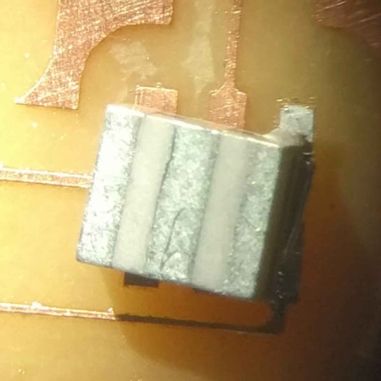
Soldering went much faster this time. I tried to remember all of the issues that we had talked about previously, and had almost no problems. There was one key exception. While soldering on the resonator, I went about it as usual, adding some solder to the pad and then heating the solder up to tac down a corner before attempting to solder the other two pads. I managed to tac it down, but it was lopsided, so I attempted to pivot it into position while keeping the solder fluid. To my surprise, as I was manipulating the resonator, it had lifted the copper trace off of the board! My best guess is that I didn't completely melt the solder, so when I lifted the resonator, it took the trace up with it too. A combintion of the particular pad being somewhat longer and thinner probably also played a role. I didn't want to restart the process, so I just decided to solder on (pun intended), taking extra care with the other two pads to make sure the component was held securely in place before attempting to fix the lifted pad. After I finished soldering the PCB, with great nervousness, I checked the connections with a multimeter, and thankfully they all held. Next was to program the board.
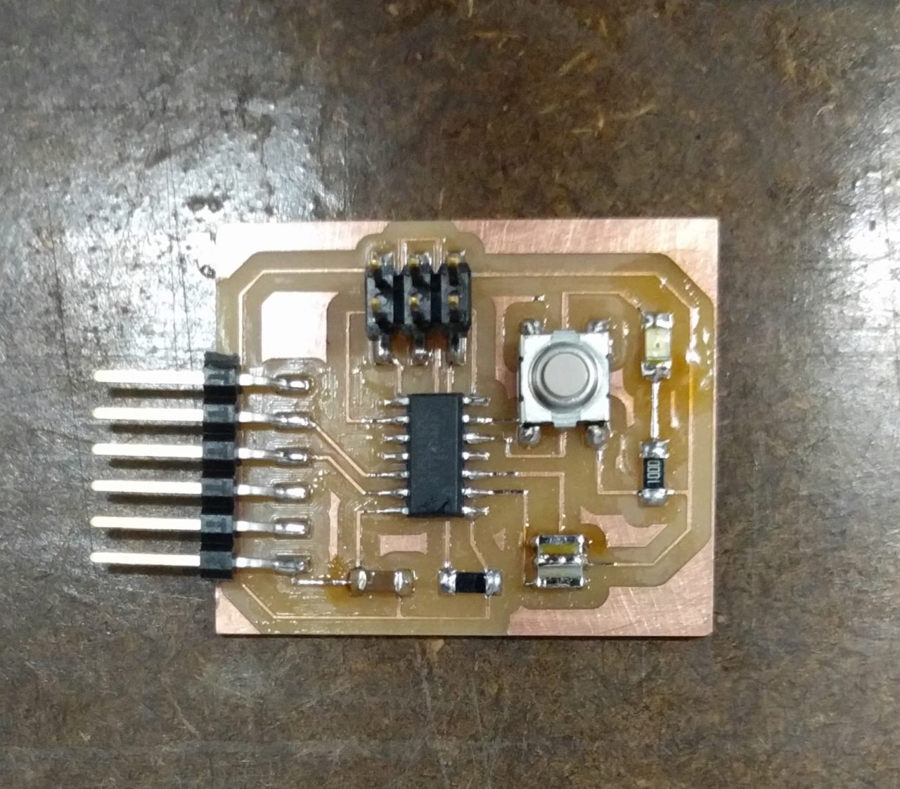
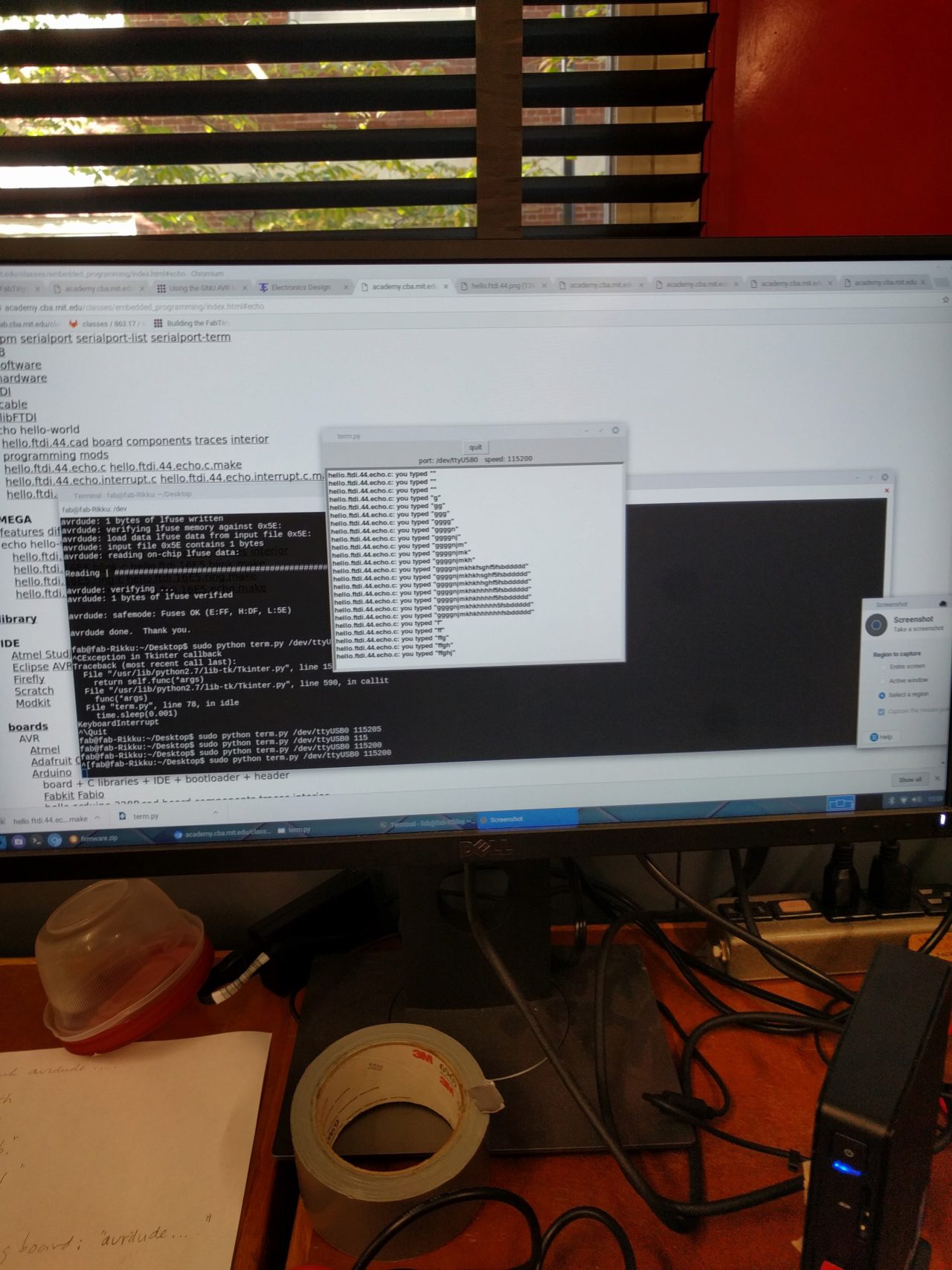
For programming, I had no idea what to do. Luckily, Brian was there and able to help me. We downloaded Neil's code for the board as well as the associated make file. We ran make -f "argument" twice where the argument was first the make file and then the fuses for the board. I'm not totally sure what the the code is doing exactly, but Brian reassured me that we would get to that in the embedded programming section in a few weeks. We next emulated a terminal using term.py. To test the board, we typed random letters, and it would say which letters we'd typed. To reset, we simply unplugged the board and reconnected it.
Special thanks to Brian, Dixon, and Rob for their help and insight!