Week 3: Electronics Fabrication
This week, we were exposed to electronics and specifically electronics fabrication. Rather than designing our own electronics or digitally-controlled devices, however, we were given the schematics for an AVR ISP programmer that we’ll use to program boards going forward and were asked to build the board. The fab techniques were 1. small-scale machine milling and 2. soldering, allowing us transform a stock copper-covered substrate into a small micro-controller controlled board.
I’ll give some high-level summary of what all of this refers to in the rest of the writeup!
PCBs, single-PCB microcontrollers, the possibilities (for embedding) are endless
A printed circuit board (PCB) drives all things digital, supporting circuit components soldered to tracks or traces that have been cut out of some conductor like copper sitting on an insulating substrate. In class, we whipped through basics of PCB machining and materials and talked about the assignment: building (though not yet totally from scratch) a programmer that will in the coming couple of weeks program other boards that will be embedded in different devices (i.e. an in-system programmer or ISP).
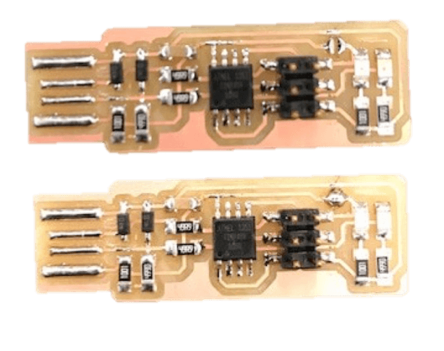
We’d be building our ISP with a ATtiny45, an adorable 8-bit microcontroller from Atmel’s family of AVR microcontrollers. While the week’s focus was on fab techniques (we haven’t written our own software for the ATtiny yet), I spent some time reading through source code – microcontroller programming is fun and is a fantastic way to spend some time close to hardware. I’ll stop there on all of that… we’ll be doing a ton on the software of embedded systems.
For what it’s worth, FabTinyISP are the instructions for the fab class itself on building this week’s ISP. This week, unlike others, we were following a straight-forward (reduced ;) ) instruction set.
Making
My making followed closely from the FabTinyISP site above. At a high level, building the FabTinyISP was as simple as…
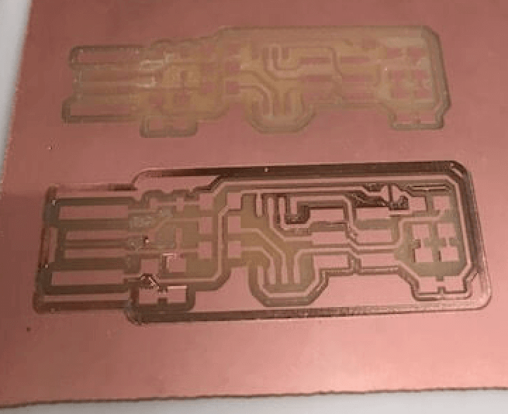
…removing copper to expose traces or tracks in a piece of printed circuit board stock…

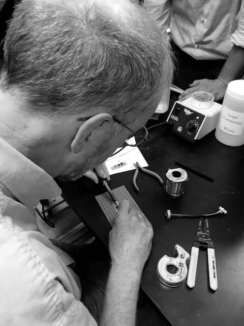
…and soldering components according to the schematic.
A few different things I documented…
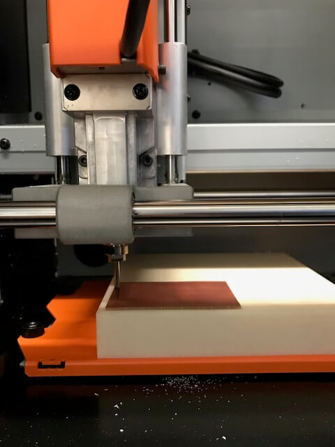
In the image below, a slab of PCB stock is still affixed to the CNC bed. You can see the cut traces, but you can also see that both the 1/64” endmill and 1/32” endmill have had a go here. The first time I ran the SRM-20, I didn’t realize the defaults for Prof Gershenfeld’s driver mods were’s setting the endmill deep enough to see the substrate underlying the copper. That would’ve been something to apply a current to.
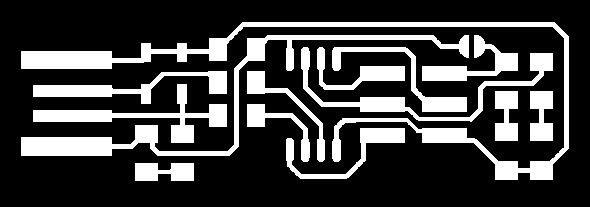
The step illustrated in the image below I found fairly compelling. The board had a different architecture when it was a programmee (without the soldered jump) from when it was a programmer (with the soldered jump). Details are documented in the instructions!