During this week, I learned to use EAGLE to remake the hello-world board, and then adding a button, an LED and its accompanying resistor. My board, in the end, did not work, but I did learn a lot to pay attention to during the process.
I first imported the fab library to EAGLE, and then found all of the needed components. Because I was not familiar with some of the names of the components, I spent sometime looking for the name either in the code or in the production image.
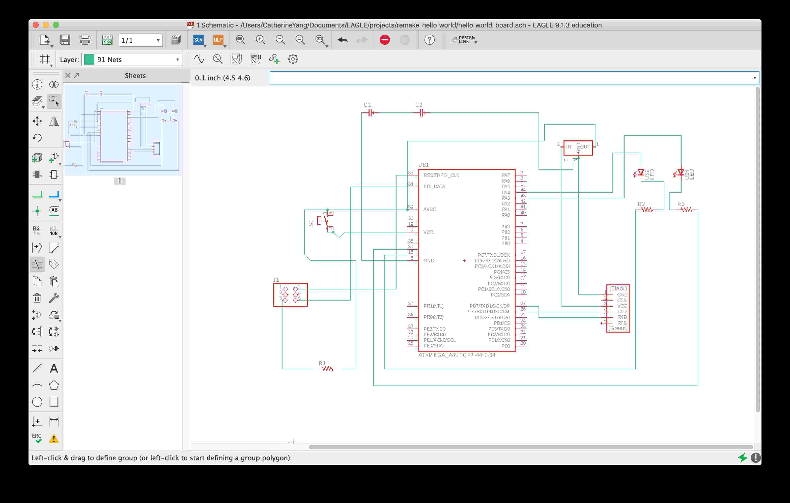
I then arranged the layout of the schematic.
Looking back, I did make some mistakes or some complication:
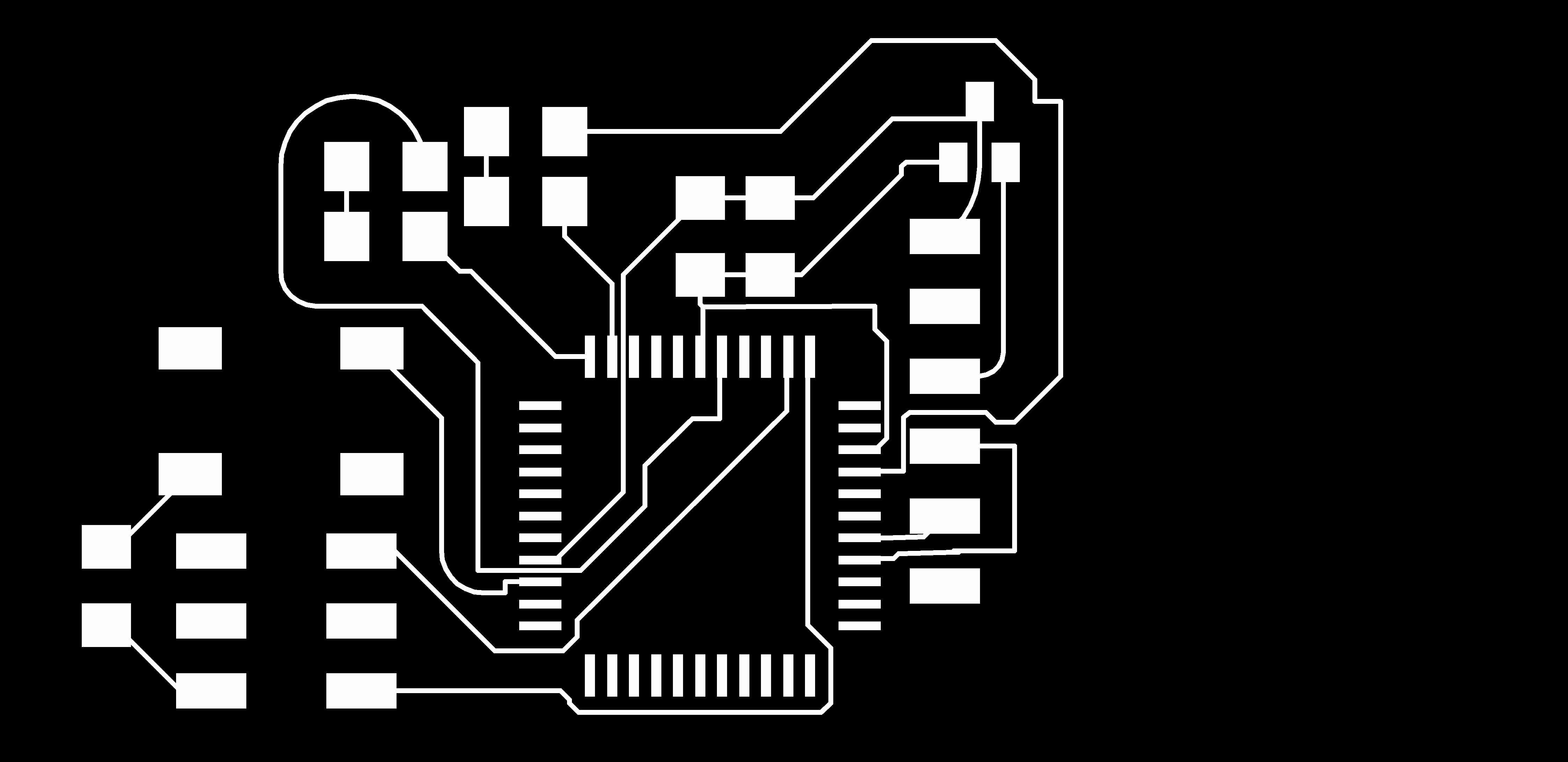
Next, I went to the board layout to route the board. What I did not but should have done at the beginning was to define the design rules. The wire was set at 0.16mm thick, and the pads were seated as 20mm. However, because I did not set up at the beginning, some of my routes were too close to each other. The routing process was a lot of rotation and moving around, as I was trying to make it as compact as possible. I did expected all my vias to be extremely thin. Also, routing the Vias under the components was super cool
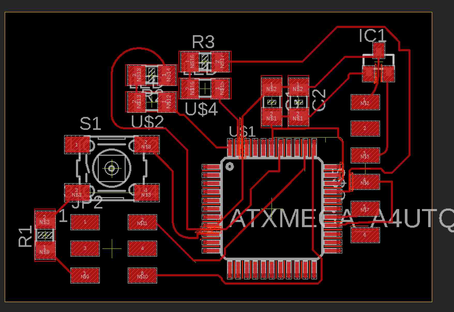
Because of the thin wires, the outcome does have two sections that I later discovered was the failing part of the board. At the top right part, where there is a via under the regulator, the route is connected to the in and out pads. At the middle right part, one of the 6 pin pads is also connected to a via. Both of them happened because I did not consider the huge difference between the default setting and the settings of our machine.

As I tried to make the board as compact as possible, the soldering becomes harder than I expected. Because some of the Vias are really close to the pads, I need to apply minimum amount of the solder on them. Also, the small “mega component” has so many tiny “legs” that I need to solder. Thus, I am not sure if I did the right thing when I soldered them.
Furthermore, because the 6 pins are not close to the edge enough to be connected flatly, I connected them by fixing them to stand with an angle.
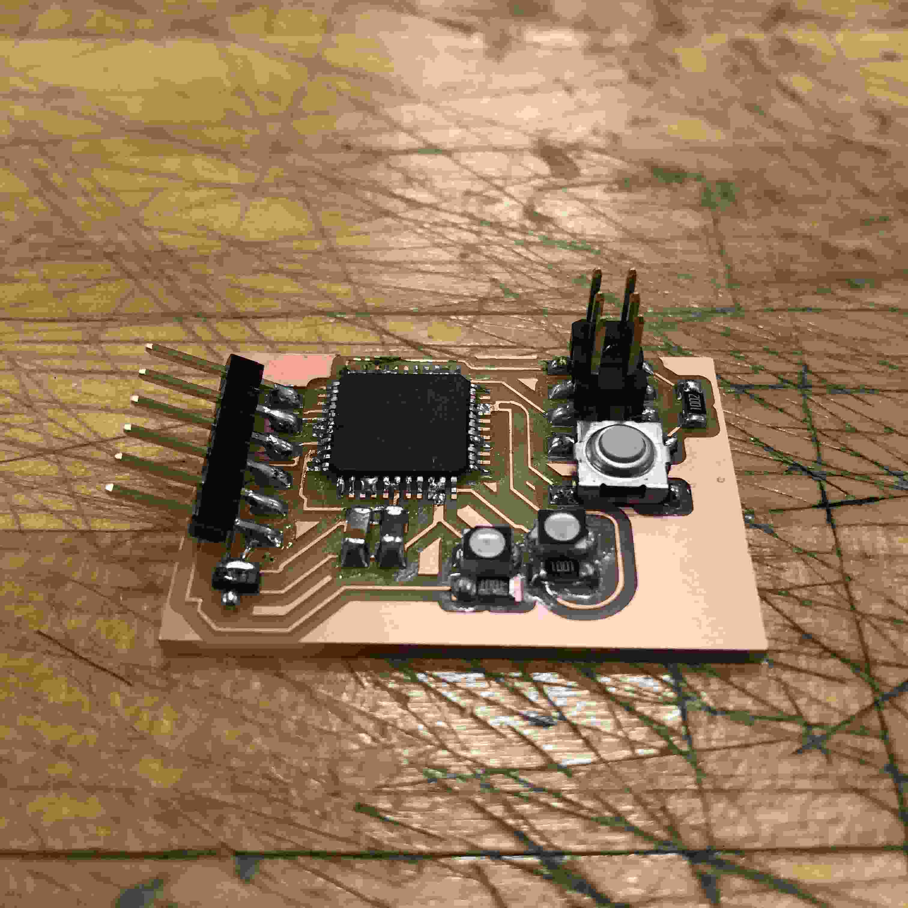
I connected it to the computer, and it does not work :(((( I will remake the board and then the improve the followings: