MAS:863 HOW TO MAKE (ALMOST) ANYTHING 2018: Casey Tang
––––––
WEEK 5: Electronics design
Assigment: redraw the echo hello-world board, add (at least) a button and LED (with current-limiting resistor)
I tried various PCB design programs and ended up using Eagle for it's integration with Fusion.
I attended the recitation and semi-learned how to use the digital voltmeter and the oscilloscope. The next day I attended office hours with a T.A that transformed into a tutorial on how to create the PCB design from beginning to end since everyone who attended did not have any experience in the process. The T.A ended up teaching us the 'Ground Plane' method as he believed this allowed for a cleaner board because there were fewer components to connect through trace.
After the tutorial I spent several hours trying to recreate it and could not connect the ground to the plane. It ended up being because I had labeled the ratsnest as ground instead of GND that would reference all the GND components on the board.
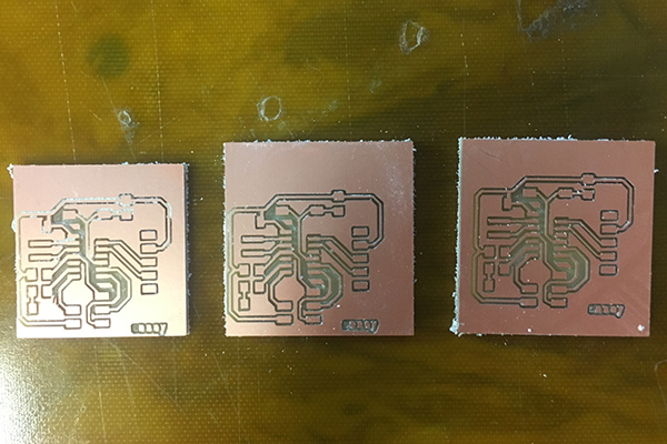
The following day I spent many hours with several students finishing the schematic and attempting to mill. The milling, however, was unsuccessful. In the 1st attempt, the mill went off the board. In the 2nd attempt, we used a bigger board and got through all the traces. The computer froze and we had to restart it. At this point in the process, I realized because we are doing the 'Ground plane' method the PNGs we had exported could be wrong. I submitted an issue in the tracker asking the T.A the proper image for exporting to mill if we are grounding to plan. After restarting we proceeded to do the outlines. For some reason when doing the outline the mill broke through the board and went off the path and cut across the board through the traces. The next day we attempted to mill again. This time the trace came out too thin. Someone from CBA recommended we change our trace from 16mil to 18mil.
I successfully milled my trace but the outline was off from the image and I had to manually move the X,Y in Mods.Apparently, if the mill is moving inaccurately it might have been improperly stopped before. You can try to reset Mods and/or Mod server.
The following instructions were created from a combinition of notes and my experiences from the faliures.
To draw your schematics...
-
Get and input libraries
- Go to the gitlab.cba.mit eagle library and download eagle-fab.lbr and eagle_png.py
- Move files into your your Eagle Document Library
-
Start new project
- Open Eagle and go to the sub-directory 'projects' under 'Projects' and make a new project and name it 'Hello World'
- Double click the file to turn it on and now the status indicator on the right should be green.
- Right click and select 'New schematic'
-
Create Grid and add components
- Create grid with size: 50. You can size the alt 0.05 for more refine work.
- Add Eagel.fab library
- Now that we added the correct library. We need to add parts from that library into our schematic. When you search for parts you will need to add an asterisks at the beginning and end of the part you are looking for i.e *LED*. You can also reference the echo schematic and photo of the complete echo board.
- Add the following pieces to your schematic:
- ATTINY44-SSU
- XTAL1
- RES-US1206
- CAP-US1206K
- (J1 ISP)
- FTDI-SMD-HEADER (also known as J2 FTD1)li>
- 6MM Switch
- Resistor
- LED
You can either interface with the program through the GUI or through the input command field. I was taught to interact with the program through commands and created my schematic using this method.
-
Connect the components
- Type Net then click and drag out the connections from the pins
- Click the connection and name them. Make sure you name the connection congruent to the function i.e Miso and Mosie.
- Change value of the resistor to 1
- Make sure the capacitor is closer to the Micro-controller
- Connect resistor to LED. Layout the signal to LED to ground.
-
Layout out your board and route the components
- Group your components and move them on the board
- Start with the micro controller unit (MCU)
- Move capacitor (C1) next to MCU
- Route the components to another
- Now that the components are connected you can draw the outline. Type line and draw a rectangle. Shift+tap with two fingers to change the corner type. Type ratsnest and name the signal GND to ground the GND.
- Type Dim and delete the board borders and redraw a new border with the polygon tool around the ground plane.
Type Edit. Brd to go to the board view. Before you start drawing your trace set your DRC clearance and type to 18mil. Keep in mind the following when you draw your traces: all yellow lines should be close as possible, minimize routing, start with components that need to be closer to each other, don't draw any right angles, use the alt (smaller grid) to move the trace.
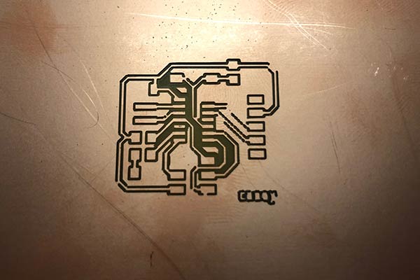
- Export image
- Type 'disp none top', type Export image, check monocrome box and set dpi as 1000. Do the same for the outline.Type 'disp non dim' to get to your outline. With retina machines you will have to half the size but keep the dpi as 1000
- Mill it
- Programs>>Open server program>>Roland>>mill>>MDX-20>>PCB
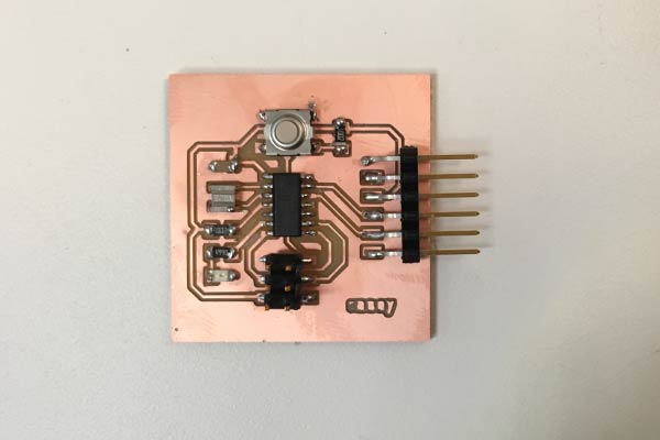
The finished board